Ultra-wideband optical perfect absorber and preparation method thereof

An ultra-broadband and absorber technology, applied in the optical field, can solve the problems of narrow wavelength range, inability to further expand the absorption bandwidth, difficult multi-band optical resonance absorption, etc., to achieve the effect of ultra-broadband and perfect optical absorption

Inactive Publication Date: 2018-03-13
JIANGXI NORMAL UNIV
View PDF9 Cites 8 Cited by
  • Summary
  • Abstract
  • Description
  • Claims
  • Application Information

AI Technical Summary

Problems solved by technology

[0004] The Chinese invention patent discloses a titanium nitride-based solar selective absorption coating, but the absorption spectrum range of the absorption coating is limited to the visible-near infrared band, and the wavelength range with high absorption efficiency is narrow and the structure is complex. Structural units such as thermal body, anti-reflection layer and absorption layer
However, based on the multi-layer structure characteristics of the inventive system, it is difficult to produce multi-band optical resonance absorption, because the absorption bandwidth cannot be further expanded, and an ultra-broadband optical perfect absorber covering the ultraviolet-visible-near-infrared band cannot be realized.

Method used


Image

  • Ultra-wideband optical perfect absorber and preparation method thereof
  • Ultra-wideband optical perfect absorber and preparation method thereof
  • Ultra-wideband optical perfect absorber and preparation method thereof

Examples


preparation example Construction

[0050] In order to achieve the above object, the present invention also provides a preparation method of an ultra-broadband optical perfect absorber, the preparation method specifically comprising:

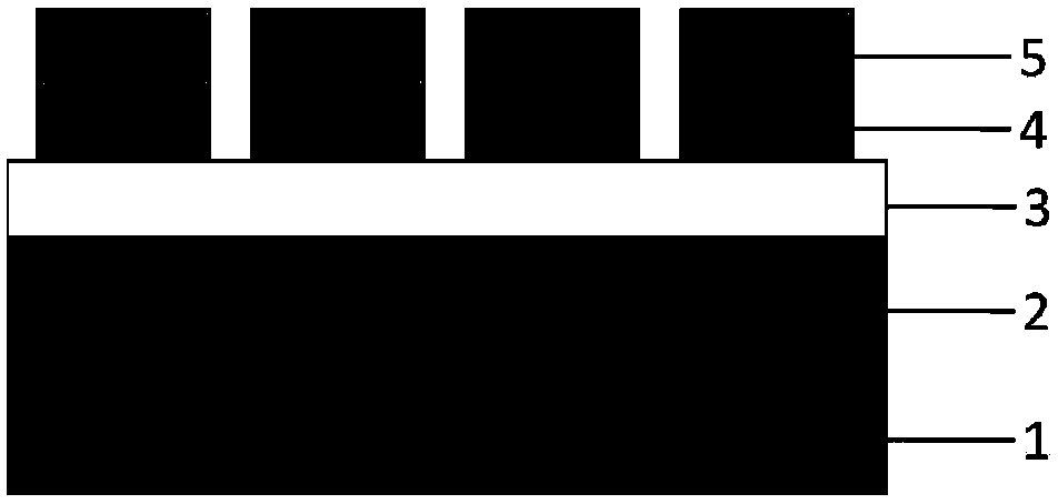
[0051] Prepare a titanium nitride film layer 2 on the substrate 1;

[0052] Depositing a dielectric film layer 3 on the upper surface of the titanium nitride film layer 2 by physical deposition;

[0053] Depositing a titanium nitride film layer on the upper surface of the dielectric film layer 3 by physical deposition;

[0054] Depositing a titanium oxide film layer on the upper surface of the titanium nitride film layer by physical deposition method;

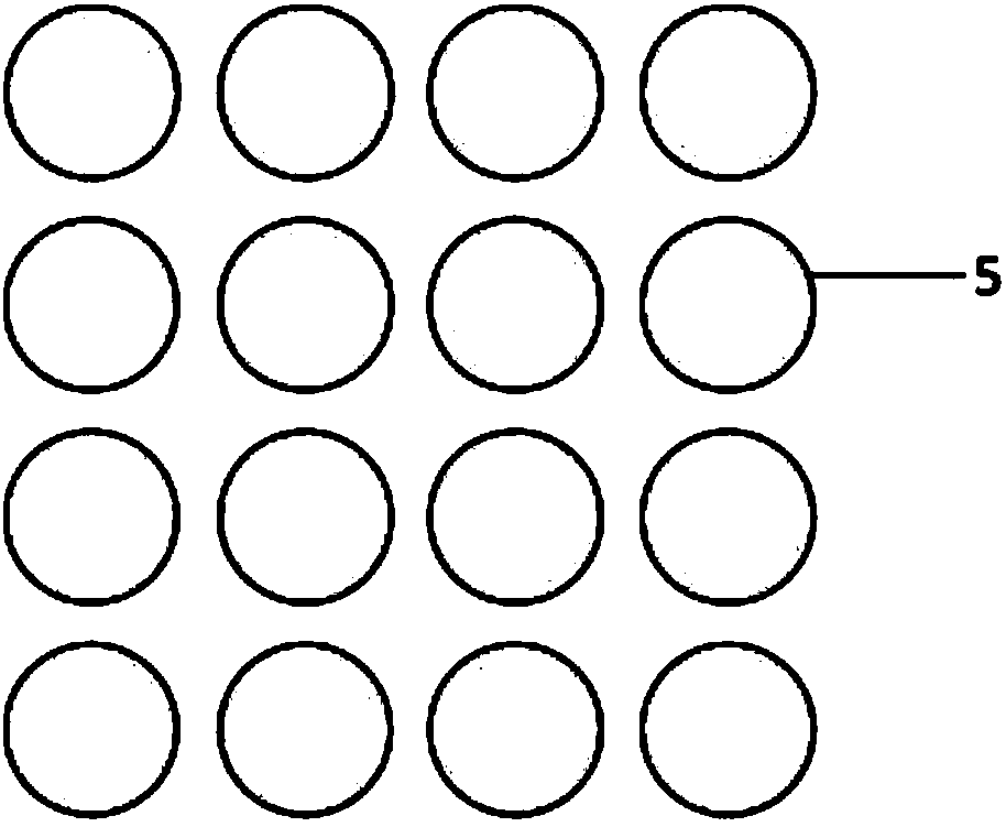
[0055] The titanium nitride film layer and the titanium oxide film layer are etched simultaneously to obtain the titanium nitride particle array 4 and the titanium oxide particle array 5 .

[0056] Optionally, the method for preparing the titanium nitride film layer 2 on the substrate 1 is a chemical growth method or a physical dep...

Embodiment 1

[0060] An ultra-broadband optical perfect absorber, including a substrate 1, the material of the substrate 1 is a silicon wafer, and a titanium nitride film layer 2, a dielectric film layer 3 and a nitrogen film layer are sequentially arranged on the substrate 1 from bottom to top. Titanium oxide-titanium oxide structural layer;

[0061] The thickness of the titanium nitride film layer 2 is 100 nanometers, the material of the dielectric film layer 3 is silicon dioxide, and the thickness of the dielectric film layer 3 is 50 nanometers; the thickness of the titanium nitride-titanium oxide structural layer is 50 nm.

[0062] The titanium nitride-titanium oxide structural layer includes a titanium nitride particle array 4 and a titanium oxide particle array 5, the titanium nitride particle array 4 is arranged on the upper surface of the dielectric film layer 3, and the titanium oxide particle array 5 is arranged on the upper surface of the titanium nitride particle array 4 .

[...

Embodiment 2

[0067] An ultra-broadband optical perfect absorber, including a substrate 1, the material of the substrate 1 is quartz, and the substrate 1 is sequentially provided with a titanium nitride film layer 2, a dielectric film layer 3 and a nitride film layer from bottom to top. Titanium-titanium oxide structural layer;

[0068] The thickness of the titanium nitride film layer 2 is 250 nanometers, and the material of the dielectric film layer 3 is silicon dioxide, and the thickness of the dielectric film layer 3 is 50 nanometers; the thickness of the titanium nitride-titanium oxide structural layer is 50 nm.

[0069] The titanium nitride-titanium oxide structural layer includes a titanium nitride particle array 4 and a titanium oxide particle array 5, the titanium nitride particle array 4 is arranged on the upper surface of the dielectric film layer 3, and the titanium oxide particle array 5 is arranged on the upper surface of the titanium nitride particle array 4 .

[0070] Such ...


PUM

PropertyMeasurementUnit
thicknessaaaaaaaaaa
thicknessaaaaaaaaaa
thicknessaaaaaaaaaa

Abstract

The invention discloses an ultra-wideband optical perfect absorber and a preparation method thereof. The ultra-wideband optical perfect absorber comprises a substrate, the substrate is provided with atitanium nitride film layer, a dielectric film layer and a titanium nitride-titanium dioxide structural layer in sequence from bottom to top, the titanium nitride-titanium dioxide structural layer comprises a titanium nitride particle array and a titanium dioxide particle array, the titanium nitride particle array is arranged on the upper surface of the dielectric film layer, and the titanium dioxide particle array is arranged on the upper surface of the titanium dioxide particle array. Ultra-wideband absorption with the coverage of ultraviolet-visible-near-infrared wavebands is realized withthe combination of the titanium nitride particle array and the titanium dioxide particle array through good absorption effect of lights with different wavelengths by titanium nitride and titanium dioxide materials.

Description

technical field [0001] The invention relates to the field of optics, in particular to an ultra-broadband optical perfect absorber and a preparation method thereof. Background technique [0002] Since 2008, the research on electromagnetic wave perfect absorber or optical perfect absorber has received extensive attention from researchers at home and abroad. In the structure, the electromagnetic resonance phenomenon realizes that the structure has neither reflection (reflectance close to 0) nor transmission (transmittance 0) at the resonant wavelength, so that according to absorption A=1-R-T (where A represents the absorption rate, R Represents the reflectivity, T represents the transmittance) definition can get the perfect absorption of the absorptivity A close to 100%, in the three-layer electromagnetic resonance structure system or metamaterial system based on metal-dielectric (or insulating material)-metal realizes from the microwave Perfect absorption response from freque...

Claims


Application Information

Patent Timeline
Patent Type & Authority Applications(China)
IPC IPC(8): G02B5/00
CPCG02B5/003
Inventor 刘正奇陈检周进刘晓山刘桂强
Owner JIANGXI NORMAL UNIV
Why Eureka
Try Eureka