Top gate self-alignment metal oxide semiconductor TFT and manufacturing method therefor

A technology of oxide semiconductor and fabrication method, applied in semiconductor/solid-state device manufacturing, semiconductor device, transistor and other directions, can solve the problems of unstable TFT operation, easy to be affected by voltage on other charged structure layers, etc., and achieve good working stability performance, improve working stability, and avoid the effect of floating gate effect

Inactive Publication Date: 2018-03-13
SHENZHEN CHINA STAR OPTOELECTRONICS SEMICON DISPLAY TECH CO LTD
View PDF9 Cites 39 Cited by
  • Summary
  • Abstract
  • Description
  • Claims
  • Application Information

AI Technical Summary

Problems solved by technology

[0007] Since metal oxide semiconductors are more sensitive to light, the threshold voltage of metal oxide semiconductor TFTs will be significantly negatively shifted after metal oxide semiconductors are exposed to light. An existing improved method is to use metal oxide semiconductor materials under the active layer The metal light-shielding layer is set to eliminate the negative drift of the TFT threshold voltage caused by light, but the metal light-shielding layer will also produce some bad effects, such as the floating gate effect. The floating gate effect refers to: because the metal light-shielding layer corresponds to the It is set under the source layer, so it is equivalent to a bottom gate. Although the metal light-shielding layer is not connected to other charged structural layers in the TFT structure, it is easily affected by the voltage on other charged structural layers, thus carrying various voltages. , because the metal light-shielding layer has a variable voltage, the threshold voltage of the TFT will continue to change when it is working, resulting in unstable TFT operation

Method used


Image

  • Top gate self-alignment metal oxide semiconductor TFT and manufacturing method therefor
  • Top gate self-alignment metal oxide semiconductor TFT and manufacturing method therefor
  • Top gate self-alignment metal oxide semiconductor TFT and manufacturing method therefor

Examples


Embodiment Construction

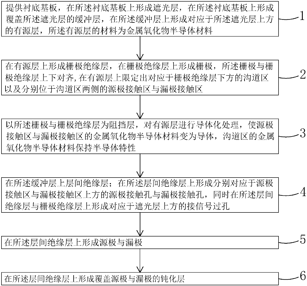
[0043] In order to further illustrate the technical means adopted by the present invention and its effects, the following describes in detail in conjunction with preferred embodiments of the present invention and accompanying drawings.

[0044] see figure 1 , the invention provides a method for fabricating a top-gate self-aligned metal-oxide-semiconductor TFT, comprising the following steps:

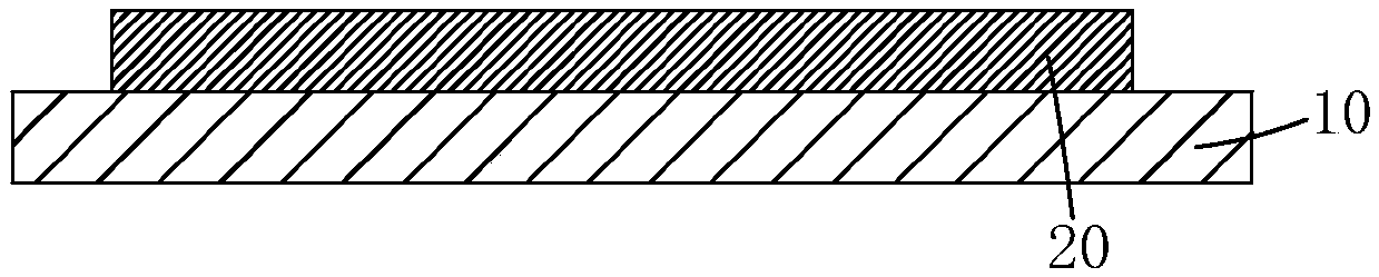
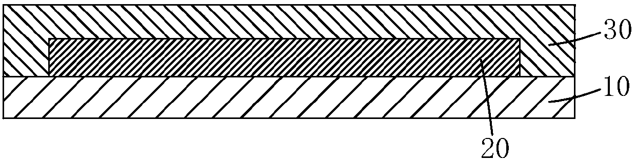
[0045] Step 1, such as figure 2 As shown, a base substrate 10 is provided, and a light shielding layer 20 is formed on the base substrate 10, such as image 3 As shown, a buffer layer 30 covering the light-shielding layer 20 is formed on the base substrate 10, as Figure 4 As shown, an active layer 40 corresponding to the top of the light shielding layer 20 is formed on the buffer layer 30 , and the material of the active layer 40 is a metal oxide semiconductor material.

[0046] Specifically, before the light-shielding layer 20 is fabricated, the base substrate 10 also needs to be c...


PUM


Abstract

The invention provides a top gate self-alignment metal oxide semiconductor TFT and a manufacturing method therefor. According to the manufacturing method of the top gate self-alignment metal oxide semiconductor TFT, a light shielding layer is arranged below an active layer, so that the active layer can be protected from light ray irradiation, and a threshold voltage negative floating phenomenon ofthe TFT can be avoided; and in addition, the light shielding layer is connected to a source, so that a stable voltage is generated on the light shielding layer to avoid generation of a floating gateeffect, thereby effectively improving operational stability of the TFT. The top gate self-alignment metal oxide semiconductor TFT, prepared by the abovementioned method, does not generate the threshold voltage negative floating phenomenon and the floating gate effect and has relatively high working stability.

Description

technical field [0001] The invention relates to the field of display technology, in particular to a top gate self-aligned metal oxide semiconductor TFT and a manufacturing method thereof. Background technique [0002] The flat panel display device has many advantages such as thin body, power saving, and no radiation, and has been widely used. Existing flat panel display devices mainly include liquid crystal display devices (Liquid Crystal Display, LCD) and organic electroluminescent display devices (Organic Light Emitting Display, OLED). [0003] LCD display devices are widely used in various consumer electronics such as mobile phones, televisions, personal digital assistants, digital cameras, notebook computers, and desktop computers due to their advantages of high image quality, power saving, thin body, and wide application range. products, becoming the mainstream of display devices. [0004] OLED display device is an active light-emitting display, which has the advantag...

Claims


Application Information

Patent Timeline
Patent Type & Authority Applications(China)
IPC IPC(8): H01L27/32H01L51/52
CPCH01L29/401H10K59/12H10K59/125H10K50/86H01L21/465H01L29/66969H01L29/7869H01L29/78633H10K59/126H10K59/131H01L29/42384H01L21/47635H01L29/78696H01L29/24H01L21/44H01L21/0273H01L21/823475
Inventor 周星宇任章淳
Owner SHENZHEN CHINA STAR OPTOELECTRONICS SEMICON DISPLAY TECH CO LTD
Why Eureka
Try Eureka