Low power consumption data acquisition transmission system based on clock chip and implementation method

A clock chip and data acquisition technology, applied in signal transmission systems, instruments, etc., to enhance intelligent control capabilities, reduce maintenance costs, and improve service life

Pending Publication Date: 2018-03-20
天津诚意创达科技有限公司
View PDF6 Cites 8 Cited by
  • Summary
  • Abstract
  • Description
  • Claims
  • Application Information

AI Technical Summary

Problems solved by technology

[0005] The invention provides a clock chip-based low-power data acquisition and transmission system and its implementation method. The invention realizes the data acquisition and transmission function based on a microcontroller chip, a sensor module, a clock chip module and a wireless communication module, and solves problems in In the case of inconvenient power supply, the battery can work effectively for a long time and realize the effective collection and transmission of data. See the description below for details:

Method used


Image

  • Low power consumption data acquisition transmission system based on clock chip and implementation method
  • Low power consumption data acquisition transmission system based on clock chip and implementation method
  • Low power consumption data acquisition transmission system based on clock chip and implementation method

Examples


Embodiment 1

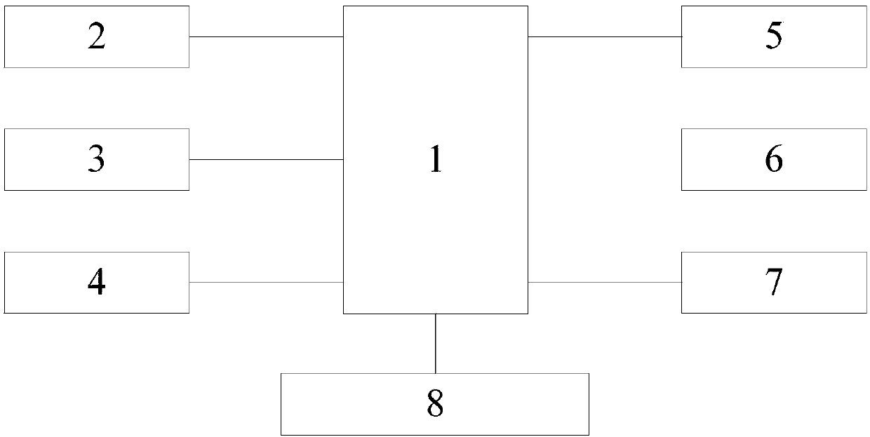
[0047] An embodiment of the present invention provides a clock chip-based low-power data acquisition and transmission system, see figure 1 The data acquisition and transmission system includes: a micro-control chip 1, a clock chip module 2, a sensor module 3, a wireless communication module 4, a storage circuit module 5, a programming circuit module 6, a crystal oscillator circuit module 7 and a power supply circuit module 8.

[0048]The micro-control chip 1 communicates with the clock chip module 2 through the I2C bus, and the interrupt pin of the micro-control chip 1 is connected with the interrupt control pin of the clock chip module 2; or I2C interface) communicates with the sensor module 3; the micro-control chip 1 communicates with the wireless communication module 4 through a serial peripheral interface (using a common UART interface); the micro-control chip 1 communicates with the wireless communication module 4 through a serial peripheral ) communicates with the stora...

Embodiment 2

[0052] Combine below figure 1 , figure 2 , image 3 The scheme in embodiment 1 is introduced in detail, see the following description for details:

[0053] see figure 1 The clock chip module 2 is used to realize the control of the micro-control chip 1, so as to realize the automatic power-on and power-off of the micro-control chip and the switching of the timing wake-up working mode.

[0054] The sensor module 3 includes: a temperature sensor, a humidity sensor, a water level sensor, a wind speed sensor, a pressure sensor, or an RFID information collector. The communication interface of the sensor module 3 can be divided into: RS485, RS232, SPI or I2C interface.

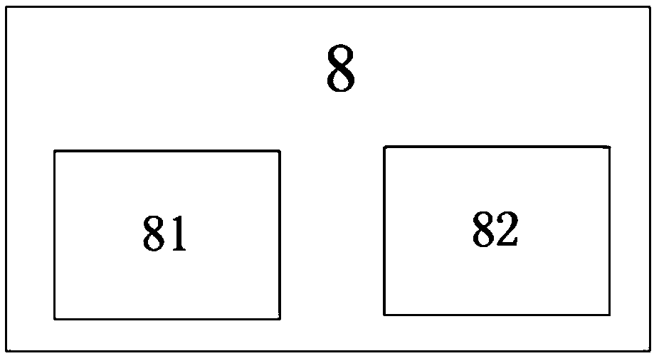
[0055] The storage circuit module 5 is used to store and read the collected information. When the device network is not connected, the collected data needs to be stored by calling the storage circuit module 5. When the network connection is successful, the micro-control chip 1 reads the data in the storage circ...

Embodiment 3

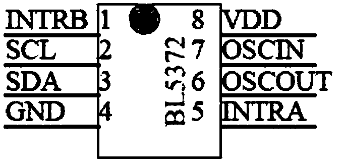
[0070] see Figure 4 , the clock chip module 2 is connected with the microcontroller chip 1 (that is, the 1st pin TNTRB, the 2nd pin SCL, the 3rd pin SDA and the 5th pin TNTRA are connected with the microcontroller chip 1); The first pin TNTRB is connected to one end of the first resistor R0; the second pin SCL of the clock chip module 2 is connected to one end of the second resistor R1; the third pin SDA of the clock chip module 2 is connected to one end of the third resistor R2 The 5th pin TNTRA of the clock chip module 2 is connected to one end of the fourth resistor R3; the 6th pin OSCOUT of the clock chip module 2 and the 7th pin OSCIN are connected with a 32.768Khz crystal oscillator; the clock chip module 2 The eighth pin VDD is respectively connected to one end of the first capacitor C0, one end of the second capacitor C1, the cathode of the first diode D0, and the cathode of the second diode D1; the anode of the first diode D0 is connected to the power supply VCC; th...


PUM


Abstract

The invention discloses a low power consumption data acquisition transmission system based on a clock chip and an implementation method. A micro control chip communicates with a clock chip module through an I2C bus; an interrupt pin in the micro control chip is connected with an interrupt control pin of the clock chip module; the micro control chip communicates with a sensor module through a universal interface; the micro control chip communicates with a wireless communication module through a serial peripheral interface; and the micro control chip communicates with a storage circuit module through the serial peripheral interface. According to the data acquisition transmission system, the micro control chip is controlled by virtue of the clock chip module, so that automatic startup and shutdown of the micro control chip and switch of timed wake-up operating modes can be realized, the lower power consumption aim of the data acquisition transmission system is achieved, energy-saving processing is realized, and the intelligent control ability of the data acquisition transmission system is enhanced. According to the lower power consumption design, the power consumption problem is solved, the service life of the product is prolonged, and the various using requirements of users are met.

Description

technical field [0001] The invention relates to the field of data acquisition, in particular to a clock chip-based low-power data acquisition and transmission system and an implementation method. Background technique [0002] Data acquisition refers to automatically collecting signals from sensors, as well as analog and digital units under test, and sending them to the host computer for analysis and processing. The collected data are various physical quantities converted into electrical signals, such as temperature, humidity, water level, wind speed, pressure, and RFID information of materials, etc., which can be analog or digital. Today, with the rapid development of the Internet industry, data collection has been widely used in the Internet and distributed fields, and important changes have taken place in the field of data collection. [0003] For many occasions where power supply is inconvenient, battery power supply is required, and power consumption control is an essen...

Claims


Application Information

Patent Timeline
Patent Type & Authority Applications(China)
IPC IPC(8): G08C17/02
CPCG08C17/02
Inventor 李承学刘毅
Owner 天津诚意创达科技有限公司
Why Eureka
Try Eureka