Unlock instant, AI-driven research and patent intelligence for your innovation.

A kind of preparation method of array substrate

An array substrate and substrate technology, applied in semiconductor/solid-state device manufacturing, semiconductor devices, electrical components, etc., can solve the problem of narrow signal line width, achieve the effects of improving yield, improving driving effect, and reducing resistance

Active Publication Date: 2020-04-17
BOE TECH GRP CO LTD +1
View PDF7 Cites 0 Cited by
  • Summary
  • Abstract
  • Description
  • Claims
  • Application Information

AI Technical Summary

Problems solved by technology

[0004] The present invention aims at the above-mentioned deficiencies existing in the prior art, and provides a preparation method of an array substrate, which is used to at least partly solve the problem of the narrow width of signal lines in the peripheral area of ​​the existing array substrate

Method used


Image

  • A kind of preparation method of array substrate
  • A kind of preparation method of array substrate
  • A kind of preparation method of array substrate

Examples


Embodiment Construction

[0042] In order for those skilled in the art to better understand the technical solution of the present invention, a method for preparing an array substrate provided by the present invention will be described in detail below with reference to the accompanying drawings.

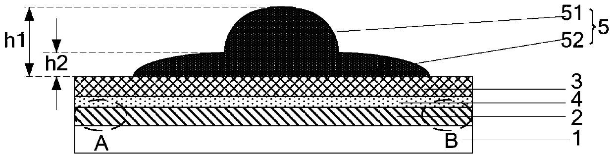
[0043] An embodiment of the present invention provides a method for preparing an array substrate, combining Figure 1a to Figure 3d As shown, the method includes: forming an active layer pattern 2 on a substrate 1 , and forming a gate film 3 on the active layer pattern 2 . Further, an insulating layer film 4 may also be formed between the active layer pattern 2 and the gate film 3 , and the insulating layer film 4 is used to isolate the active layer pattern 2 and the gate film 3 . It should be noted that the method for forming the active layer pattern 2, the gate film 3 and the insulating layer film 4 on the substrate 1 is the same as that of the prior art, and will not be repeated here.

[0044] The method a...


PUM


Abstract

The invention provides a preparation method of an array substrate. According to the method, a grid mask pattern and a signal line mask pattern are synchronously formed on a grid electrode thin film. The grid mask pattern is divided into a first region and at least one second region. The second region is located at the edge of the grid mask pattern. The thickness of the second region is smaller than the thickness of the first region and the thickness of the signal line mask pattern. In this way, in the second region without the grid mask pattern, the width of the signal line mask pattern can bekept unchanged due to the fact that the thickness of the signal line mask pattern is larger than the thickness of the second region during the forming process of a grid pattern and a lightly doped region in an area wherein an active layer pattern is formed. Accordingly, the width of a signal line pattern formed by the signal line mask pattern can be improved, so that the resistance of a signal line can be reduced. The driving effect of the array substrate is correspondingly improved. Moreover, the defect that the array substrate is poor due to disconnection of the signal line can be avoided.The yield of the array substrate is further improved.

Description

technical field [0001] The invention relates to the field of display technology, in particular to a method for preparing an array substrate. Background technique [0002] In the prior art, an active layer in a low temperature polysilicon LTPS (Low Temperature Poly-Silicon) thin film transistor includes a lightly doped region and a heavily doped region, and the heavily doped region is located at both ends of the active layer, and is connected to the source and the The drain is connected to reduce the contact resistance between the active layer and the source and drain, and the lightly doped region is located in the middle region of the active layer to reduce the leakage current between the source and the drain. The step of forming a doped region and a heavily doped region in the region of the active layer specifically includes: firstly forming a gate thin film on the substrate on which the pattern of the active layer is formed; The gate mask pattern is formed at the position...

Claims


Application Information

Patent Timeline
Patent Type & Authority Patents(China)
IPC IPC(8): H01L21/84H01L27/12H01L29/423
CPCH01L27/124H01L27/1288H01L29/42384
Inventor 晁晋予郭志轩于亚楠方业周蔡志光李付强
Owner BOE TECH GRP CO LTD