Scanning electron microscope demonstration method and device not adopting optical lens

A technology of optical lens and scanning electron microscope, applied in teaching models, educational tools, instruments, etc., can solve the problems of multiple accessories, complex lens optical path system, complex process, etc., and achieve the effect of convenient setting

Inactive Publication Date: 2018-03-23
HARBIN INST OF TECH SHENZHEN GRADUATE SCHOOL
View PDF8 Cites 6 Cited by
  • Summary
  • Abstract
  • Description
  • Claims
  • Application Information

AI Technical Summary

Problems solved by technology

[0008] It is well known that the interaction between the electron beam and the sample will produce strong radiation, so the entire electron optical system is enclosed by metal in the vacuum electron chamber and sample chamber, plus many components, using the electron microscope itself or the device that uses the electron beam for demonstration The entire imaging process cannot be visualized
[0009] At present, in the experimental teaching of undergraduates and postgraduates, the explanation of scanning electron microscope content in the course of analysis and testing technology is an important part of it, but the existing teaching often only involves theoretical teaching, which is neither vivid nor intuitive, and the classroom content The optical path diagram of the scanning electron microscope often uses optical lenses to express the focusing process of the electron beam. After learning, many students mistakenly think that optical lenses are used in scanning electron microscopes.
[0010] There is no ready-made physical teaching model of scanning electron microscope in the market. Among the existing patent applications, the device described in the application number CN201510498386.8 is actually to manufacture a complete scanning electron microscope entity, which requires a lot of accessories, complicated Technology, multi-party cooperation and high cost are not practical and cannot intuitively observe the interaction process of the converged electron beam and the sample.
The transmission electron microscope, which belongs to the electron microscope, has applied for patent numbers CN201610237039.4 and CN201610326811.X. It uses optical lenses to simulate the behavior of electron beams, but it cannot demonstrate the unique phenomena in electron optics. For example, the electron beam rotates forward in the magnetic field of the condenser. , and the optical path system using the lens is very complex, with many components and precise adjustment

Method used


Image

  • Scanning electron microscope demonstration method and device not adopting optical lens
  • Scanning electron microscope demonstration method and device not adopting optical lens
  • Scanning electron microscope demonstration method and device not adopting optical lens

Examples


Embodiment Construction

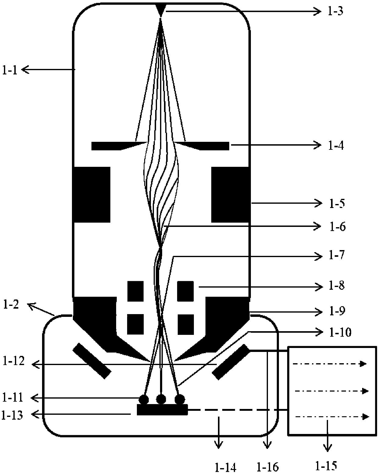
[0020] The invention provides a scanning electron microscope demonstration method that does not use optical lenses. The optical path is prefabricated into a specific shape by using light-transmitting or luminescent materials to form an optical path model, which is used in conjunction with the corresponding sample model. The attraction to demonstrate the scanning process and signal receiving process, effectively avoiding the adverse effects of using the optical lens system demonstration.

[0021] As a further improvement of the present invention, the optical path model prefabricated with light-transmitting or luminescent materials is divided into upper and lower parts. The upper optical path is made into a spiral downward shape with gradually increasing curvature and remains fixed; the lower optical path can be deflected under the action of a magnetic field, which can be used to demonstrate the process of electron beam scanning. As a further improvement of the present invention...


PUM


Abstract

The invention provides a scanning electron microscope demonstration method not adopting an optical lens. According to the method, a material is prefabricated into a light path model of a specific shape, the light path model is matched with a sample model for use, the whole process including the rotation, focusing and deflection of electron beams in the scanning electron microscope, the interactionwith the sample, and the sample collection is simulated by virtue of the mechanism of attraction for soft magnetic materials of an electromagnet, and the adverse effects caused by using the optical lens for simulation are avoided. The invention further provides a scanning electron microscope demonstration device not adopting the optical lens. The device is placed in a transparent lens cone and asample bin, the demonstrated part is convenient to observe and also is very convenient to arrange and refit. The method and the device have the beneficial effects that the whole process of imaging ofthe scanning electron microscope can be demonstrated, namely, the whole process from the generation of electron beams to signal receiving and the profound principle contained in the whole process aredemonstrated; the whole demonstration process is intuitional and visual, so that the principle is very easy to understand, and the device also has the advantages of low cost, simplicity in refitting and the like.

Description

technical field [0001] The invention relates to a scanning electron microscope, in particular to a visualized scanning electron microscope demonstration method and device. Background technique [0002] Scanning electron microscope (scanning electron microscope for short) is currently widely used in the fields of material science, environmental science, life science, electronic manufacturing, new energy, failure analysis, etc., to reflect the microscopic morphology and composition of samples and many other information. Wide range of applications. Therefore, the scanning electron microscope has become the standard equipment for research in the field of materials in major universities and scientific research institutions at home and abroad. It takes a long time for university teachers and students, scientific research and testing personnel who use this equipment to be familiar with and understand the principles and characteristics of the scanning electron microscope. Lectures ...

Claims


Application Information

Patent Timeline
Patent Type & Authority Applications(China)
IPC IPC(8): G09B23/22
CPCG09B23/22
Inventor 高尚
Owner HARBIN INST OF TECH SHENZHEN GRADUATE SCHOOL
Why Eureka
Try Eureka