OLED, display panel and display device

A light-emitting diode, an organic technology, applied in semiconductor devices, electrical components, circuits, etc., can solve the problems of increasing the driving voltage of organic light-emitting diodes, reducing the luminous efficiency and service life of organic light-emitting diodes, and increasing the energy barrier of electron transmission. Achieve the effects of improving service life and luminous efficiency, preventing accumulation, and improving voltage stability

Active Publication Date: 2018-04-06
WUHAN TIANMA MICRO ELECTRONICS CO LTD
View PDF4 Cites 9 Cited by
  • Summary
  • Abstract
  • Description
  • Claims
  • Application Information

AI Technical Summary

Problems solved by technology

The P-type organic semiconductor layer 051 of the charge generation layer 05 is in direct contact with the N-type organic semiconductor layer 052. As the cumulative operating time of the organic light-emitting diode increases, electrons are likely to flow at the interface between the P-type charge generation layer and the N-type charge generation layer. Accumulated at places, thereby increasing the energy barrier of electron transport, leading to an increase in the driving voltage of the organic light-emitting diode with this structure, and reducing the luminous efficiency and service life of the organic light-emitting diode

Method used


Image

  • OLED, display panel and display device
  • OLED, display panel and display device
  • OLED, display panel and display device

Examples


Embodiment Construction

[0049] In order to improve the voltage stability of the organic light emitting diode during long-term operation, reduce the power consumption of the organic light emitting diode, and improve the service life and luminous efficiency of the organic light emitting diode, an embodiment of the present invention provides an organic light emitting diode, a display panel and a display device. In order to make the purpose, technical solution and advantages of the present invention clearer, the following examples are given to further describe the present invention in detail.

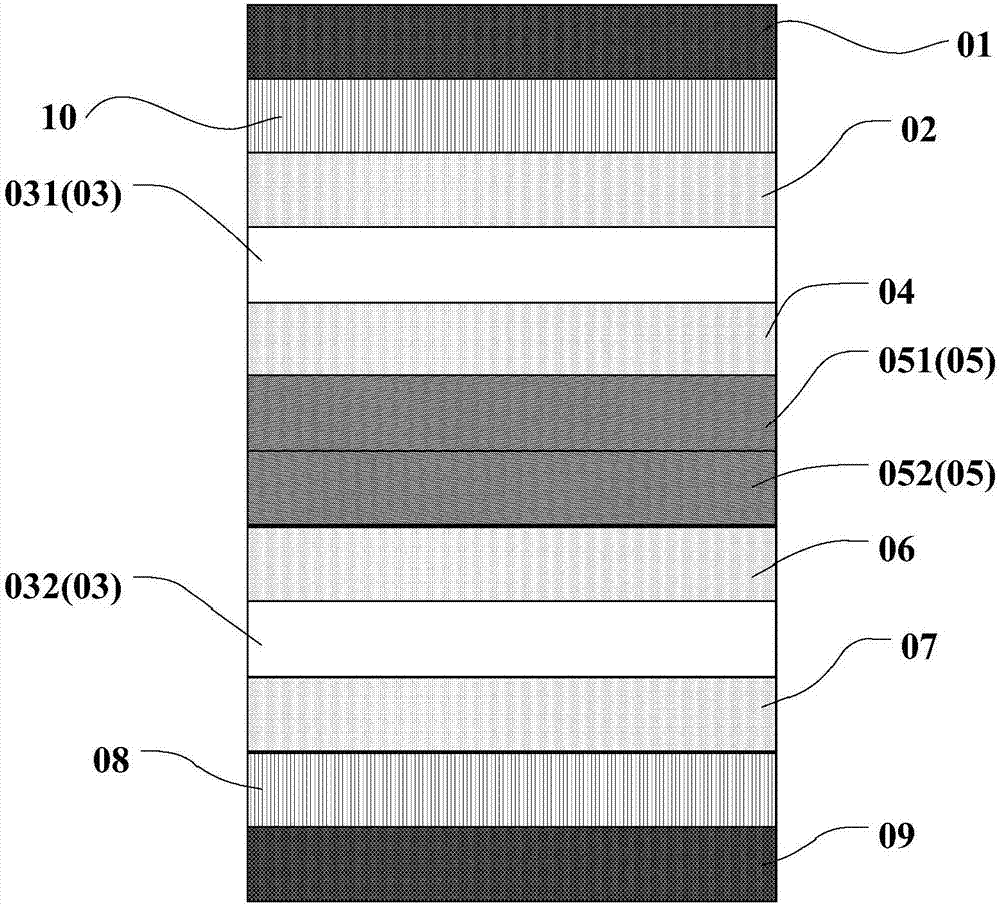
[0050] Such as figure 2 as shown, figure 2It is a schematic structural diagram of an organic light emitting diode according to an embodiment of the present invention. The organic light-emitting diode provided by the embodiment of the present invention includes: an anode 10, a cathode 1, at least two light-emitting layers 4 arranged between the anode 10 and the cathode 1, and a charge generation device arranged...


PUM


Abstract

The invention discloses an OLED, a display panel and a display device to improve the light-emitting efficiency and THE service life of the OLED. The OLED includes an anode, a cathode, at least two light-emitting layers disposed between the anode and the cathode, a charge generating layer disposed between any two adjacent light-emitting layers, a first functional layer and a second functional layer. The charge generating layer includes a first hole transport substrate, a first electron transport substrate, a first P-type semiconductor dopant, and a first N-type semiconductor dopant. The first functional layer includes a second electron transport substrate and a second N-type semiconductor dopant. The second electron transport substrate and the first electron transport substrate have the same lowest unoccupied orbital energy level. The second functional layer includes a second hole transport substrate and a second P-type semiconductor dopant. The second hole transport substrate and the first hole transport substrate have the same highest occupied molecular orbital energy level.

Description

technical field [0001] The invention relates to the field of display technology, in particular to an organic light emitting diode, a display panel and a display device. Background technique [0002] Organic electroluminescence is a phenomenon in which organic materials are excited by electric energy to emit light. Organic electroluminescent devices have low driving voltage, high luminous brightness, high luminous efficiency, wide luminous viewing angle, fast response speed, ultra-thin, light weight and compatible flexibility. Substrates and other advantages occupy an important position in the display field. [0003] Organic Light-Emitting Diode (OLED for short), as a representative product of organic electroluminescent devices, has been extensively studied. [0004] Please refer to figure 1 , a common organic light-emitting diode in the prior art includes sequentially stacked cathode 01, electron injection layer 10, first electron transport layer 02, first light-emitting l...

Claims


Application Information

Patent Timeline
Patent Type & Authority Applications(China)
IPC IPC(8): H01L51/50H01L27/32
CPCH10K59/12H10K30/865H10K50/11H10K2101/40H10K50/15H10K50/16
Inventor 舒鹏王湘成牛晶华刘营
Owner WUHAN TIANMA MICRO ELECTRONICS CO LTD
Why Eureka
Try Eureka