Interconnecting wire structure of semiconductor device and manufacturing method of interconnecting wire of semiconductor device
A manufacturing method and technology of interconnection lines, which are applied in semiconductor/solid-state device manufacturing, semiconductor/solid-state device parts, semiconductor devices, etc., can solve problems such as interconnection holes and achieve the effect of improving reliability
- Summary
- Abstract
- Description
- Claims
- Application Information
AI Technical Summary
Problems solved by technology
Method used
Image

Examples
Embodiment 1
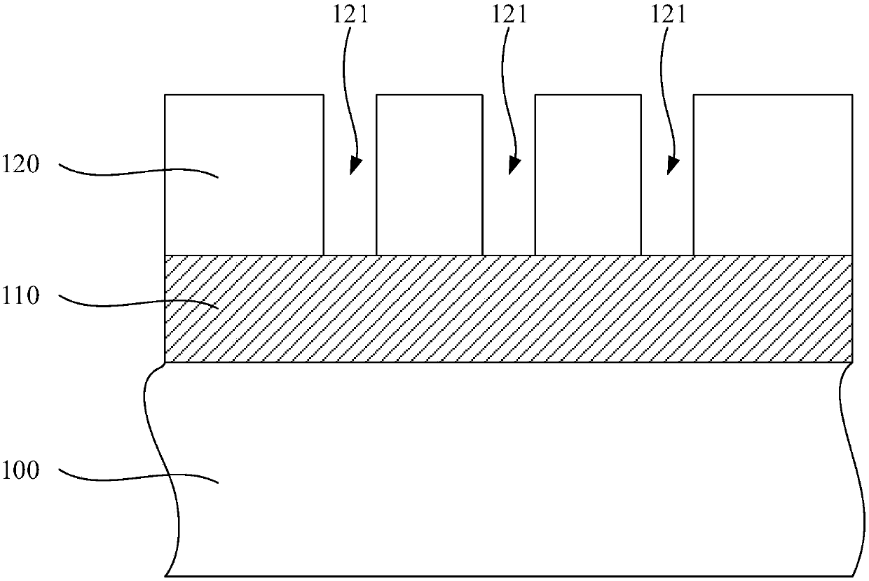
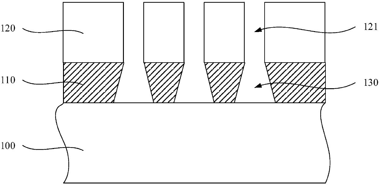
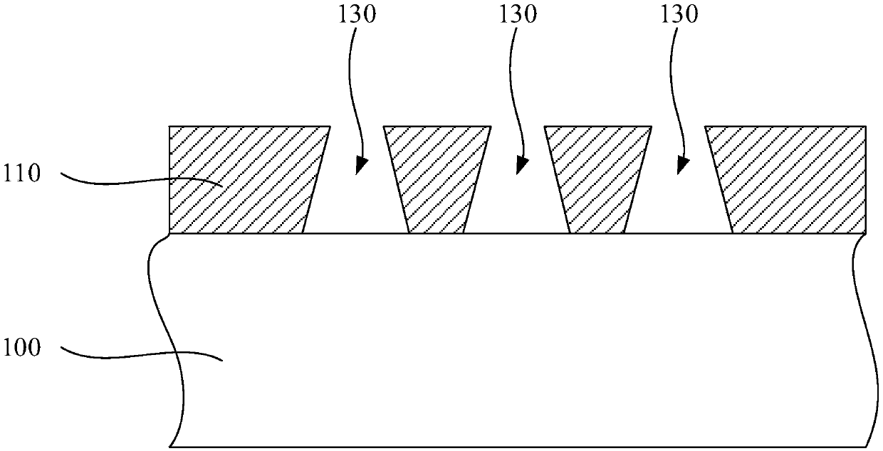
[0092] Specifically, please refer to Figure 5 to Figure 9 ,in, Figure 5 is a schematic cross-sectional view of the substrate provided in the method for manufacturing interconnection lines of a semiconductor device according to Embodiment 1 of the present invention; Figure 6 is true Figure 5 A schematic cross-sectional view of the structure shown after performing a patterned etching process; Figure 7 is in Figure 6 A schematic cross-sectional view of the structure shown after removing the patterned etch barrier layer and the passivation film; Figure 8 is in Figure 7 A schematic diagram of the structure after metal interconnection lines are formed on the shown structure; Figure 9 is in Figure 7 A schematic diagram of the structure after forming a copper seed layer and a copper electroplating layer on the shown structure.
[0093] First, if Figure 5 As shown, a substrate 200 is provided, and a dielectric layer 210 is formed on the substrate 200 . In the embodi...
Embodiment 2
[0130] Specifically, please refer to Figure 12 to Figure 16 ,in, Figure 12 is a schematic cross-sectional view of the substrate provided in the method for manufacturing interconnection lines of semiconductor devices according to Embodiment 2 of the present invention; Figure 13 is true Figure 12 A schematic cross-sectional view of the structure shown after performing a patterned etching process; Figure 14 is in Figure 13 A schematic cross-sectional view of the structure shown after removing the patterned etch barrier layer; Figure 15 is in Figure 14 A schematic diagram of the structure after metal interconnection lines are formed on the shown structure; Figure 16 is in Figure 14 A schematic diagram of the structure after forming a copper seed layer and a copper electroplating layer on the shown structure.
[0131] First, if Figure 12 As shown, a substrate 300 is provided, and a dielectric layer 310 is formed on the substrate 300 . In the embodiment of the pr...
PUM
| Property | Measurement | Unit |
|---|---|---|
| Width | aaaaa | aaaaa |
| Depth | aaaaa | aaaaa |
| Thickness | aaaaa | aaaaa |
Abstract
Description
Claims
Application Information
 - R&D Engineer
- R&D Manager
- IP Professional
- Industry Leading Data Capabilities
- Powerful AI technology
- Patent DNA Extraction
Browse by: Latest US Patents, China's latest patents, Technical Efficacy Thesaurus, Application Domain, Technology Topic.
© 2024 PatSnap. All rights reserved.Legal|Privacy policy|Modern Slavery Act Transparency Statement|Sitemap