Ultraviolet LED and preparation method
A technology of light-emitting diodes and light-emitting layers, applied in semiconductor devices, electrical components, circuits, etc., can solve the problems of limited UVC band effect, no three-dimensional light scattering structure, etc., to improve light extraction efficiency, facilitate light propagation, and facilitate lead wires Effect
- Summary
- Abstract
- Description
- Claims
- Application Information
AI Technical Summary
Problems solved by technology
Method used
Image

Examples
Embodiment Construction
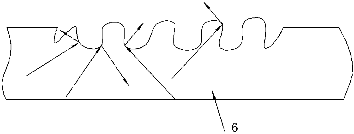
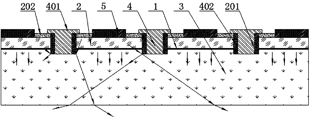
[0027] Such as figure 2 As mentioned above, it is a kind of ultraviolet light-emitting diode, including a light-emitting layer 1, a P-type layer 2 located on one side of the light-emitting layer 1, and an N-type layer 3 located on the other side of the light-emitting layer 1, and a plurality of through-holes are separated on the P-type layer 2. Holes 201, through-holes 201 are periodically and regularly distributed or randomly distributed on the P-type layer 2, the through-holes 201 are circular holes with a diameter of 200nm to 5000nm or square holes or triangular holes or hexagonal holes with a cross-sectional inscribed circle of 200nm to 5000nm , the through holes 201 can reasonably set the N electrode 4, and each through hole 201 penetrates the light-emitting layer 1 downward from the P-type layer 2, and each through hole 201 is provided with an N electrode 4, and one end of the N electrode 4 extends out of the P-type layer 2 An N-terminal electrode 401 is formed. The cro...
PUM
| Property | Measurement | Unit |
|---|---|---|
| Thickness | aaaaa | aaaaa |
| Diameter | aaaaa | aaaaa |
Abstract
Description
Claims
Application Information