

Electrostatic chuck and reaction chamber
A technology of electrostatic chuck and reaction chamber, which is applied in the direction of circuits, electrical components, electric solid devices, etc., can solve problems such as processing difficulties, achieve the effects of reducing processing difficulty, solving thermal expansion and heat insulation problems, and reducing processing difficulty
- Summary
- Abstract
- Description
- Claims
- Application Information
AI Technical Summary
Problems solved by technology
Method used
Image

Examples
Embodiment Construction
[0027] In order to enable those skilled in the art to better understand the technical solutions of the present invention, the present invention will be described in detail below in conjunction with the accompanying drawings.
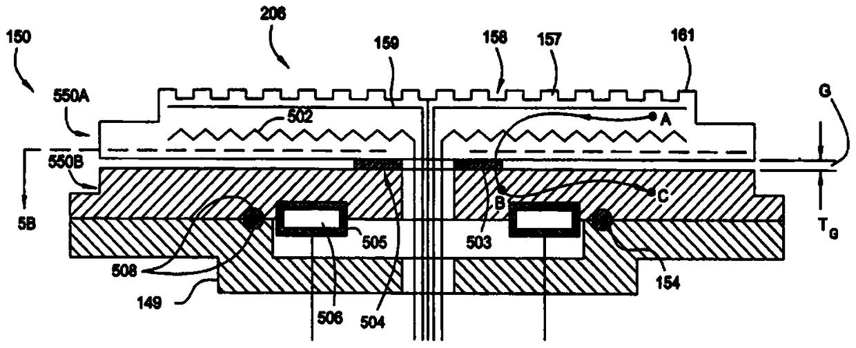
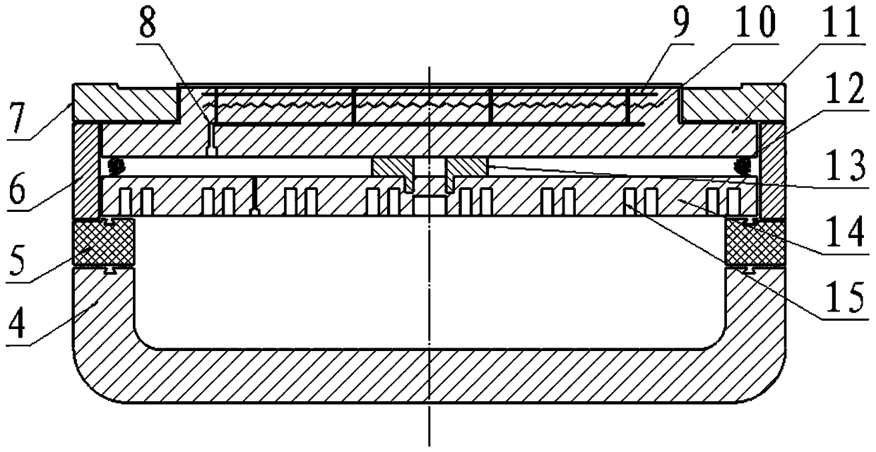
[0028] image 3 A cross-sectional view of an electrostatic chuck provided by an embodiment of the present invention. see image 3 , the electrostatic chuck includes: an electrostatic chuck assembly, a cooling element 14 , a supporting insulating element 13 and a sealing insulating element 12 . Wherein, the electrostatic chuck assembly is located above the cooling element 14 . In this embodiment, the electrostatic chuck assembly includes: a main structure 11 , an electrode 9 inside the main structure 11 and a heating component 10 . The material of the main structure 11 is ceramics, preferably alumina ceramics or aluminum nitride ceramics. Electrodes 9 and heating elements 10 are produced by printing. Preferably, the material of the electrode 9 is Mo o...
PUM
 Abstract
Description
Claims
Application Information