Methods for making an X-ray detector
An X-ray and X-ray technology, which is applied in the field of making semiconductor X-ray detectors, can solve the problems of difficult and impossible production of detectors with large areas and a large number of pixels.
- Summary
- Abstract
- Description
- Claims
- Application Information
AI Technical Summary
Problems solved by technology
Method used
Image
Examples
Embodiment Construction
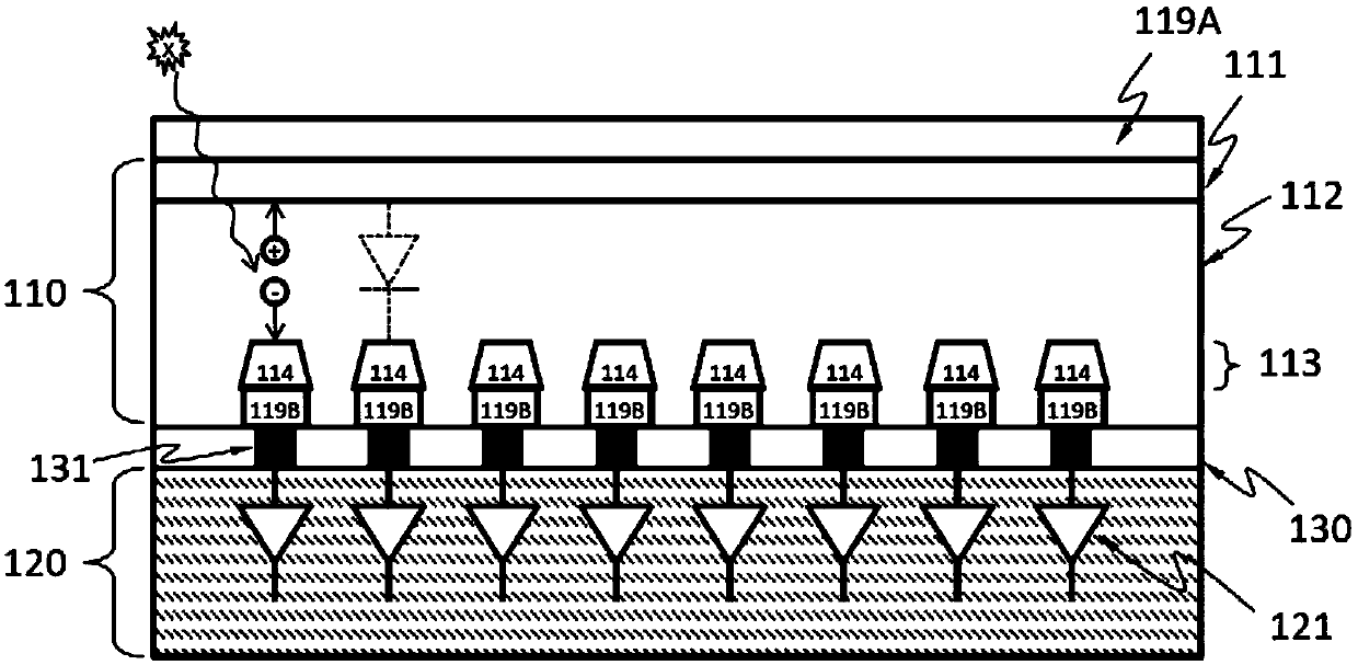
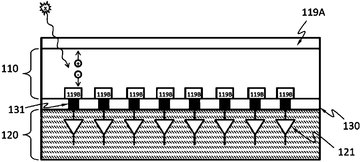
[0069] Figure 1A A semiconductor X-ray detector 100 according to an embodiment is schematically shown. The semiconductor X-ray detector 100 may include an X-ray absorbing layer 110 and an electronic layer 120 (for example, an ASIC) for processing or analyzing electrical signals generated in the X-ray absorbing layer 110 by incident X-rays. In an embodiment, the semiconductor X-ray detector 100 does not include a scintillator. The X-ray absorbing layer 110 may include semiconductor materials such as silicon, germanium, GaAs, CdTe, CdZnTe or combinations thereof. Semiconductors can have high mass attenuation coefficients for x-ray energies of interest.
[0070] as in Figure 1B As shown in the detailed cross-sectional view of the detector 100, according to an embodiment, the X-ray absorbing layer 110 may include one or more discrete regions 114 formed from the first doped region 111 and the second doped region 113 One or more diodes (for example, p-i-n or p-n). The second d...
PUM
 Abstract
Description
Claims
Application Information
 - R&D Engineer
- R&D Manager
- IP Professional
- Industry Leading Data Capabilities
- Powerful AI technology
- Patent DNA Extraction
Browse by: Latest US Patents, China's latest patents, Technical Efficacy Thesaurus, Application Domain, Technology Topic, Popular Technical Reports.
© 2024 PatSnap. All rights reserved.Legal|Privacy policy|Modern Slavery Act Transparency Statement|Sitemap|About US| Contact US: help@patsnap.com


