Heat radiation gain face-to-face semiconductor assembly with heat radiation base and making method thereof

A manufacturing method and semiconductor technology, which are applied in the fields of semiconductor/solid-state device manufacturing, semiconductor devices, and semiconductor/solid-state device components, etc., can solve the problems of high cost, complex process, and poor thermal environment of components.

Inactive Publication Date: 2018-04-24
BRIDGE SEMICON
View PDF8 Cites 0 Cited by
  • Summary
  • Abstract
  • Description
  • Claims
  • Application Information

AI Technical Summary

Problems solved by technology

Although it does not require the formation of through-silicon vias (TSVs) in the stacked chips, the TSVs in the interposer used to provide electrical routing between chips will lead to complex manufacturing processes, low production yields, and high costs
In addition, since semiconductor chips are prone to performance degradation at high operating temperatures, if the face-to-face stacked chips are not properly dissipated, the thermal environment of the components will deteriorate, resulting in immediate failure during operation

Method used


Image

  • Heat radiation gain face-to-face semiconductor assembly with heat radiation base and making method thereof
  • Heat radiation gain face-to-face semiconductor assembly with heat radiation base and making method thereof
  • Heat radiation gain face-to-face semiconductor assembly with heat radiation base and making method thereof

Examples


Embodiment 1

[0123] Figure 1-18 In the first embodiment of the present invention, it is a diagram of a method of manufacturing a face-to-face semiconductor component, which includes a first routing circuit 21, a first semiconductor chip 22, a series of vertical connectors 24, a sealing material 25 and a heat conducting plate 31 and a second semiconductor chip 36.

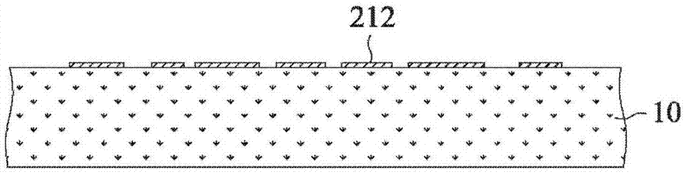
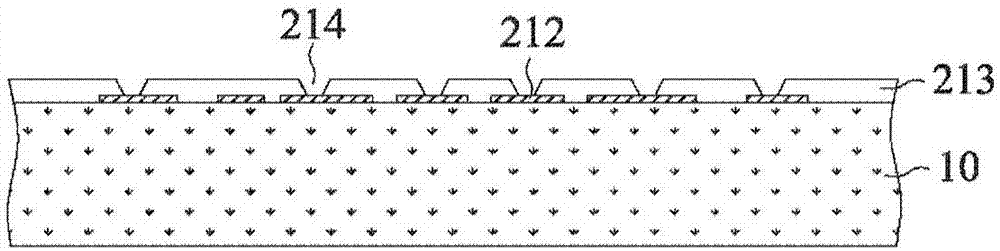
[0124] figure 1 It is a cross-sectional view of the routing lines 212 formed on the sacrificial carrier 10 , wherein the routing lines 212 are formed by metal deposition and metal patterning processes. In this figure, the sacrificial carrier 10 is a single-layer structure. The sacrificial carrier 10 is usually made of copper, aluminum, iron, nickel, tin, stainless steel, silicon or other metals or alloys, but any other conductive or non-conductive material can also be used. In this embodiment, the sacrificial carrier 10 is made of ferrous material. Routing lines 212 are typically made of copper and can be patterned deposite...

Embodiment 2

[0149] Figure 20-26 In the second embodiment of the present invention, it is a diagram of a face-to-face semiconductor assembly manufacturing method for attaching another heat sink to the first semiconductor chip.

[0150] For the purpose of brief description, any descriptions in the above-mentioned embodiment 1 that can be used for the same application are incorporated here, and it is not necessary to repeat the same descriptions.

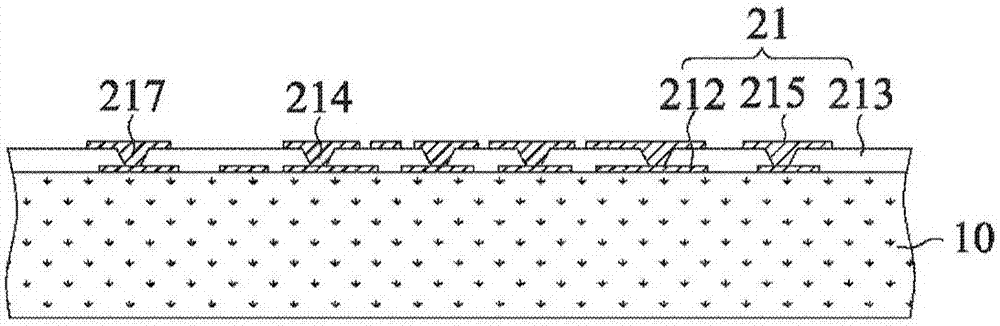
[0151] Figure 20 for solder balls 242 placed in Figure 4 A cross-sectional view of the first routing circuit 21 . The solder balls 242 are disposed on the edge area of ​​the outer surface of the first routing circuit 21 and contact the first wire 215 to serve as the vertical connection elements 24 surrounding the first semiconductor chip 22 .

[0152] Figure 21 It is a cross-sectional view of the heat sink 23 attached to the first semiconductor chip 22 . The heat sink 23 can be made of any material with high thermal conductivity, such as ...

Embodiment 3

[0162] Figure 28-35 It is a diagram of a fabrication method of a face-to-face semiconductor component with an external routing circuit in the third embodiment of the present invention.

[0163] For the purpose of brief description, any descriptions in the above embodiments that can be used for the same application are incorporated here, and the same descriptions do not need to be repeated.

[0164] Figure 28 To form the sealing material 25 in Figure 4 A cross-sectional view of the first routing circuit 21 and the first semiconductor chip 22 in FIG. The sealing material 25 covers the first routing circuit 21 and the first semiconductor chip 22 from above, and surrounds, conformally covers and covers the sidewall of the first semiconductor chip 22 .

[0165] Figure 29 It is a cross-sectional view of forming the blind hole 256 in the sealing material 25 . The blind holes 256 are aligned with selected positions of the first wires 215 of the first routing circuit 21 , and ...


PUM


Abstract

A face-to-face semiconductor assembly of the invention is characterized in that a sealing device is electrically coupled to and superimposed on a heat radiation gain device; the sealing device has a first semiconductor element which is surrounded by a series of vertical connectors in a sealing material; and the heat radiation gain device has a second semiconductor chip which is accommodated in a recess of a heat conduction plate. The first and two semiconductor chips are connected to two opposite sides of a first routing circuit in a face-to-face manner, and are further electrically connectedto the vertical connectors via the first routing circuit. The heat conduction plate has a heat radiation base which provides a way for heat radiation of the second semiconductor chip. The first routing circuit can provide primary fan-out routing for the first and two semiconductor chips, and the vertical connectors can provide electrical contacts for next-level connection.

Description

technical field [0001] The invention relates to a face-to-face semiconductor component and its manufacturing method, in particular to a face-to-face semiconductor component in which two semiconductor devices are connected face to face by means of a dual routing circuit, and one of the devices is provided with an external contact terminal. Background technique [0002] The market trend of multimedia devices tends to be faster and thinner. One of the methods is to interconnect two chips in a face-to-face manner so that the routing distance between the two chips is the shortest. Since the stacked chips can be directly transmitted to each other to reduce the delay, the signal integrity of the components can be greatly improved and additional energy consumption can be saved. Therefore, the face-to-face semiconductor device can exhibit almost all the advantages of 3D IC stacking without forming costly through-silicon vias (Through-Silicon Via) in the stacked chips. For example, ...

Claims


Application Information

Patent Timeline
Patent Type & Authority Applications(China)
IPC IPC(8): H01L23/367H01L23/488H01L21/60
CPCH01L24/16H01L24/81H01L23/367H01L2224/16148H01L2224/81238H01L2924/181H01L2224/16H01L2924/00012
Inventor 林文强王家忠
Owner BRIDGE SEMICON
Why Eureka
Try Eureka