Vertical pHEMT transistor structure and switch chip

A transistor and isolation layer technology, applied in semiconductor devices, electric solid state devices, semiconductor/solid state device components, etc., can solve the problem of low isolation, and achieve the effect of short interconnection distance, high integration and strong control ability

Active Publication Date: 2021-02-26
成都挚信电子技术有限责任公司
View PDF12 Cites 0 Cited by
  • Summary
  • Abstract
  • Description
  • Claims
  • Application Information

AI Technical Summary

Problems solved by technology

[0012] (1) A single microwave switch based on a pHEMT structure transistor, the principle is that the gate barrier controls the current on and off between the source and the drain, which inherently has the problem of low isolation

Method used


Image

  • Vertical pHEMT transistor structure and switch chip
  • Vertical pHEMT transistor structure and switch chip
  • Vertical pHEMT transistor structure and switch chip

Examples


Embodiment 2

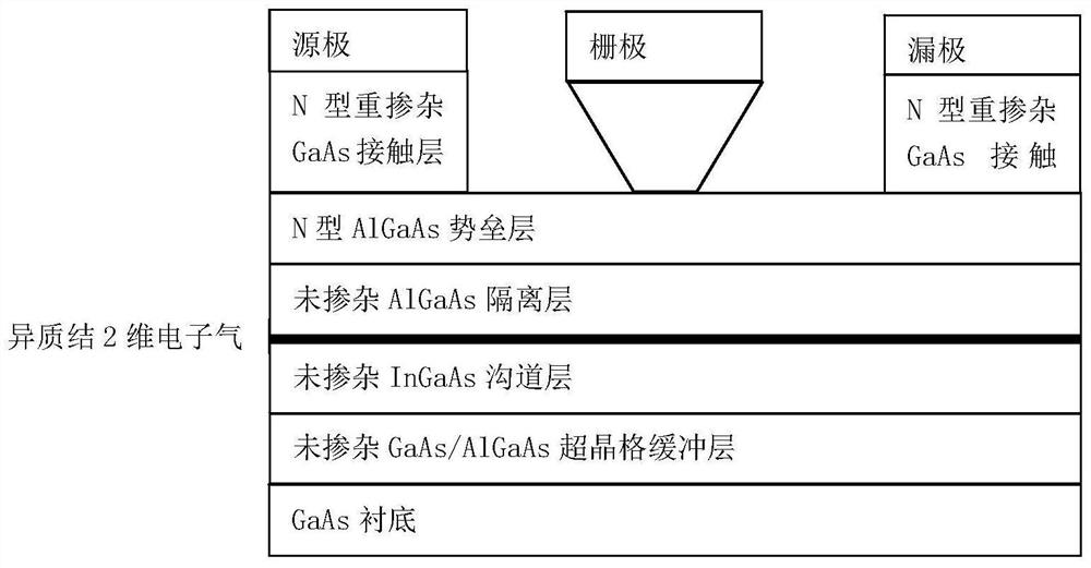
[0046] This embodiment discloses a vertical pHEMT microwave transistor structure, the transistor structure includes:

[0047] Around the metallized through hole, an undoped GaAs / AlGaAs superlattice buffer layer, an undoped InGaAs channel layer, an undoped AlGaAs isolation layer and an N-type AlGaAs barrier layer are sequentially arranged from the inner layer to the outer layer, The axial direction of the metallized through hole is the same as the normal direction of the substrate; the source, gate, and drain are set on the side wall of the N-type AlGaAs barrier layer, and the source and drain are set on the side wall of the N-type AlGaAs barrier layer. The GaAs contact layer is heavily doped such that the 2D electron gas is distributed axially around the metallized via. The metallized through hole forms a columnar structure along the normal direction of the substrate. Correspondingly, each layer structure around the metallized through hole also forms a columnar structure, and ...

Embodiment 3

[0049] This embodiment discloses a vertical stacking structure of pHEMT transistors, which is formed by vertically stacking the vertical pHEMT microwave transistor structures in the above-mentioned embodiments on the substrate, and each adjacent two layers of vertical pHEMT microwave transistors include an upper layer transistor and a lower layer Transistors, upper layer transistors and lower layer transistors are vertically stacked (that is, stacked along the normal direction of the substrate), a second isolation layer is provided between the upper layer transistors and the lower layer transistors, and metallized vias for conduction and heat conduction are provided vertically through the second isolation layer . The structure of the upper layer transistor and the lower layer transistor adopts the above-mentioned pHEMT microwave transistor structure respectively. It should be noted that although the vertical pHEMT microwave transistor structure of the above-mentioned embodiment...


PUM


Abstract

The invention discloses a vertical pHEMT transistor structure and a switch chip. The transistor comprises a buffer layer, a channel layer, a first isolation layer and a barrier layer which are sequentially arranged around a metallized through hole from the inner layer to the outer layer, the metallized through hole, the buffer layer, the channel layer, the first isolation layer and the barrier layer are each of a columnar structure, the axial direction of the metallized through hole is the same as the normal direction of a substrate, a source electrode, a grid electrode and a drain electrode are arranged on the barrier layer, the source electrode, the grid electrode and the drain electrode are horizontally or vertically arranged, and the grid electrode surrounds the columnar side wall fora circle during vertical arrangement. The switch chip is formed by connecting a plurality of vertical pHEMT transistors in series or in parallel in the vertical direction. The transistor and the switch chip provided by the invention have the characteristics of high isolation, large power capacity, small size, good integration, low power consumption, high efficiency and good broadband characteristic.

Description

technical field [0001] The invention relates to the field of semiconductor chips, in particular to a vertical pHEMT transistor structure and a switch chip formed by a vertical pHEMT transistor stack structure. Background technique [0002] Microwave switches are widely used in modern communication systems such as transceiver modules. There are two technologies for existing microwave switches: one is a mechanical switch, which uses electricity to control the on-off of the mechanical arm to control the switch of the microwave channel; the other is a chip switch, which uses electricity to control the on-off of the transistor in the chip to control the microwave channel. switch. [0003] Advantages of mechanical switches over chip switches: high isolation, which can reach more than 60dB, while chip switches can only reach about 20dB. Therefore, mechanical switches are widely used in instrumentation and other fields that require high isolation, high sensitivity, and precision m...

Claims


Application Information

Patent Timeline
Patent Type & Authority Applications(China)
IPC IPC(8): H01L29/778H01L29/423H01L23/367H01L23/373H01L25/07
CPCH01L29/7788H01L29/42316H01L23/367H01L23/3736H01L25/074
Inventor 黄永锋殷玉喆何力刘伟
Owner 成都挚信电子技术有限责任公司
Why Eureka
Try Eureka