
LED packaging method and structure

A technology of LED packaging and LED chips, which is applied in the direction of semiconductor devices, electrical components, circuits, etc., can solve the problems of affecting heat dissipation effect, small heat capacity of metal heat dissipation substrate, and easy deformation, so as to increase heat dissipation effect, improve luminous dispersion, reduce cost effect

Inactive Publication Date: 2018-04-27
XIAN CREATION KEJI CO LTD
View PDF6 Cites 0 Cited by
  • Summary
  • Abstract
  • Description
  • Claims
  • Application Information

AI Technical Summary

Problems solved by technology

[0005] 1. At present, most of the chips are packaged on a thin metal heat dissipation substrate. Because the metal heat dissipation substrate is thin, the heat capacity is small, and it is easy to deform, the contact between it and the bottom surface of the heat sink is not close enough to affect the heat dissipation effect.
[0006] 2. Since the light emitted by the LED light source is generally distributed in a divergent manner, that is, the Lambertian distribution, this causes the illumination brightness of the light source to be insufficiently concentrated, and generally requires secondary shaping through an external lens to meet the lighting needs of specific occasions, which increases production costs.

Method used


Image

  • LED packaging method and structure
  • LED packaging method and structure
  • LED packaging method and structure

Examples


Embodiment 1

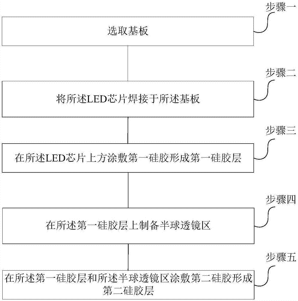
[0046] See figure 1 , figure 1 A schematic flow chart of an LED packaging method provided by an embodiment of the present invention, including:

[0047] Step 1. Select the heat dissipation substrate;

[0048] Step 2, welding the LED chip to the heat dissipation substrate;

[0049] Step 3, coating the first silica gel on the LED chip to form a first silica gel layer;

[0050] Step 4, preparing a hemispherical lens area on the first silica gel layer;

[0051] Step 5: Coating second silica gel on the first silica gel layer and the hemispherical lens area to form a second silica gel layer.

[0052] Wherein, the heat dissipation substrate is a copper material heat dissipation substrate.

[0053] Specifically, the refractive index of silica gel in the first silica gel layer, the second silica gel layer and the hemispherical lens area increases sequentially.

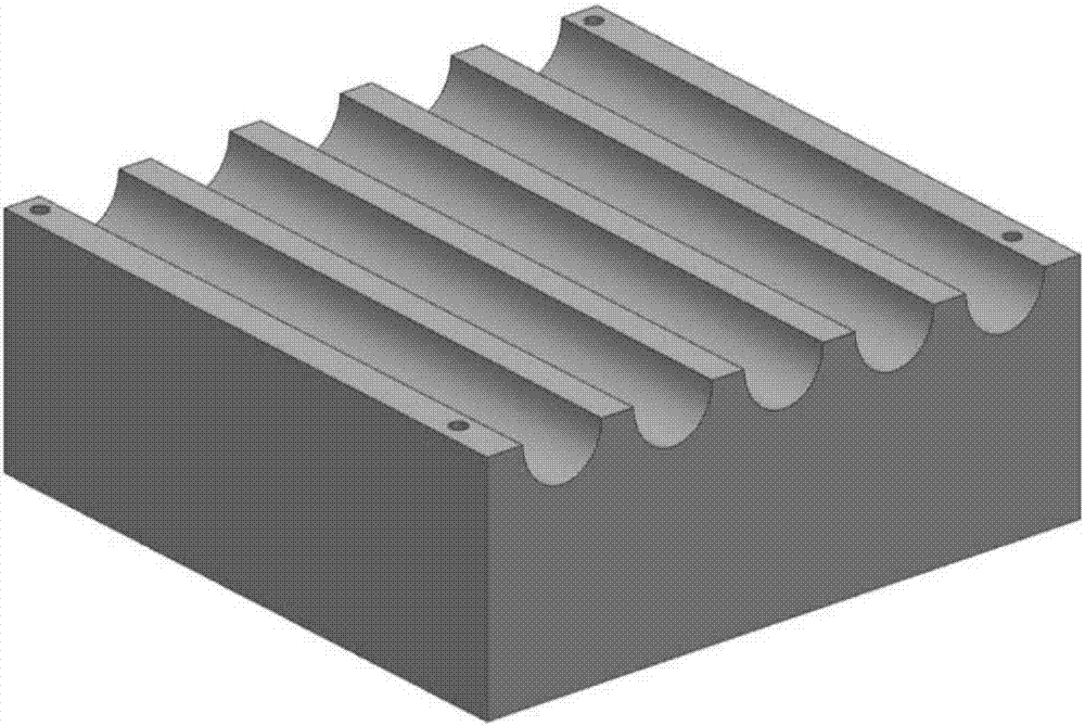
[0054] Specifically, see figure 2 , figure 2 It is a schematic diagram of a heat dissipation substrate of an LED pa...

Embodiment 2

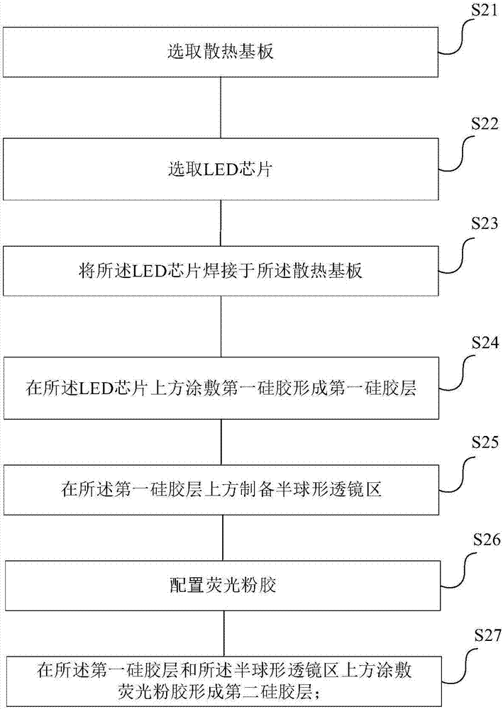
[0072] Please refer to image 3 , image 3 The flow chart of the LED packaging method provided by another embodiment of the present invention, this embodiment is based on the above-mentioned embodiments, and the LED packaging method of the present invention is described in detail as follows. Specifically, include the following steps:

[0073] S21, selecting a heat dissipation substrate;

[0074] S22, selecting LED chips;

[0075] S23. Welding the LED chip to the heat dissipation substrate;

[0076] S24, coating the first silica gel on the LED chip to form a first silica gel layer;

[0077] S25. Prepare a hemispherical lens area above the first silica gel layer;

[0078] S26, configuring fluorescent powder glue;

[0079] S27. Apply phosphor glue on the first silica gel layer and the hemispherical lens region to form a second silica gel layer; to complete the LED package.

[0080] Specifically, step S21 may include:

[0081] S211, selecting a heat dissipation substrate a...

Embodiment 3

[0116] Further, please refer to Figure 6 , Figure 6 It is a schematic diagram of an LED package structure provided in yet another embodiment of the present invention. The LED package structure provided in this embodiment is prepared by the method provided in the above embodiment. Specifically, the LED packaging structure includes: an LED heat dissipation substrate 31 , a first silica gel layer 32 , a hemispherical lens area 33 and a second silica gel layer 34 from bottom to top.

[0117] Wherein, the LED heat dissipation substrate 31 includes a heat dissipation substrate and LED chips disposed on the heat dissipation substrate.

[0118] Specifically, the first silica gel layer 32 is silica gel without phosphor powder, and the second silica gel layer is silica gel containing phosphor powder.

[0119] Further, the hemispherical lens area 33 includes several rectangular or diamond-shaped silica gel hemispheres evenly distributed, and the silica gel in the silica gel hemispher...


PUM

PropertyMeasurementUnit
Thicknessaaaaaaaaaa

Abstract

The invention relates to an LED packaging method and an LED packaging structure. The LED packaging method comprises the steps of: step 1, selecting a heat-dissipating substrate; step 2, welding an LEDchip to the heat-dissipating substrate; step 3, coating a first silica gel layer on the LED chip; step 4, preparing a hemispherical lens region on the first silica gel layer; step 5, and coating a fluorescent powder adhesive on the first silica gel layer and in a hemispherical cavity region to form a second silica gel layer. The LED packaging method and the LED packaging structure provided by theinvention adopt the structures of the first silica gel layer, the hemispherical lens region and the second silica gel layer; a lens is formed in the silica gel by utilizing the features of differenttypes of silica gel in the structures of the first silica gel layer, the hemispherical lens region and the second silica gel layer and different refractive indexes of the fluorescent powder adhesive,thus the problem of scattered light emission of the LED chip is improved, and the light emitted by means of a light source can be more concentrated; meanwhile, the refractive indexes of the first silica gel layer, the second silica gel layer and the hemispherical lens region are increased in sequence, thereby ensuring that the LED chip can illuminate more through packaging materials.

Description

technical field [0001] The invention belongs to the technical field of LED packaging, in particular to an LED packaging method and structure. Background technique [0002] At the end of the last century, the breakthrough of III-V compound semiconductors represented by GaN-based materials in the field of blue light chips brought about a revolution in lighting. The symbol of this revolution is the high-power light-emitting diode (Light-Emitting Diode, LED) Semiconductor lighting technology (Solid State Lighting, SSL) as the light source. [0003] LED has the characteristics of long life, high luminous efficiency, good color rendering, safety and reliability, rich colors and easy maintenance. Under the background of increasingly serious environmental pollution, climate warming and increasingly tense energy sources, semiconductor lighting technology developed based on high-power LEDs has been recognized as one of the most promising high-tech fields in the 21st century. This is...

Claims


Application Information

Patent Timeline
IPC IPC(8): H01L33/00H01L33/48H01L33/50H01L33/54H01L33/56H01L33/58H01L33/64
CPCH01L33/0075H01L33/48H01L33/504H01L33/54H01L33/56H01L33/58H01L33/641
Inventor 张亮
Owner XIAN CREATION KEJI CO LTD
Features
  • Generate Ideas
  • Intellectual Property
  • Life Sciences
  • Materials
  • Tech Scout
  • Unparalleled Data Quality
  • Higher Quality Content
  • 60% Fewer Hallucinations
Learn More