Carrying device for special-shaped wafers

A carrier device and chip technology, applied in the direction of electrical components, semiconductor/solid-state device manufacturing, circuits, etc., can solve problems such as inappropriate devices, irregular actions, and high risks, so as to improve efficiency, save resources, and improve work efficiency Effect

Pending Publication Date: 2018-05-04
CHINA ELECTRONICS TECH GRP NO 46 RES INST
View PDF8 Cites 0 Cited by
  • Summary
  • Abstract
  • Description
  • Claims
  • Application Information

AI Technical Summary

Problems solved by technology

At present, such special-shaped products are in the laboratory stage. During the processing or process, the standard wafer carrying device or manual operation are often used, which can easily cause samp

Method used


Image

  • Carrying device for special-shaped wafers
  • Carrying device for special-shaped wafers
  • Carrying device for special-shaped wafers

Examples


Embodiment

[0018] Example: refer to Figure 1 to Figure 8 , using this device to determine the polar surface of a square cadmium sulfide (CdS) wafer with polarity, the specific steps are as follows:

[0019] (1) Place the CdS crystal ingot on the cutting machine to cut the wafer or large-area sample, and the cutting thickness is controlled at 600-700μm;

[0020] (2) Cut the wafer / large-area sample into square pieces of 15㎜х15㎜, with a cutting error of ±0.5mm;

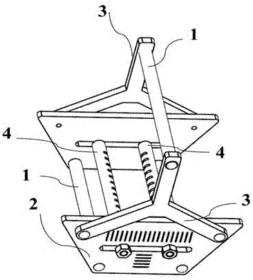
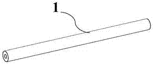
[0021] (3) Adjust the distance between the support rods 4 of the carrying device through the side plate track 2-1, and control it between 10mm-12mm;

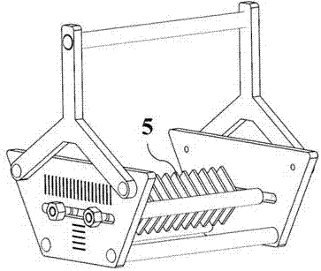
[0022] (4) Place the cut square piece 5 vertically in the groove 4-1 on the pole 4 of the carrying device, and the sharp corner of the square piece is lower than the bottom edge of the pole 4;

[0023] (5) Prepare hydrochloric acid in the container: corrosion solution with deionized water volume ratio of 1:5; concentration of hydrochloric acid is 36%-38%; corrosion at room tempera...


PUM


Abstract

The invention discloses a carrying device for special-shaped wafers. The carrying device comprises connecting rods, side plates, lifting bars and supporting rods, wherein the two connecting rods are connected with and fix the two side plates, one connecting rod is connected with and fixes the upper ends of the lifting bars, and the lower ends of the lifting bars are fixed on the side plates respectively; side plate tracks for adjusting space between the two supporting rods and bearing wafers in different sizes are arranged on the side plates, and two ends of each supporting rod are fixed in the side plate tracks; side plate vertical scales for precision control of a wafer corrosion area and side plate horizontal scales for precision adjustment of the supporting rod space are formed in theside plates, and a plurality of grooves for carrying to-be-corroded wafers are formed in the two supporting rods respectively. Flexible adjustment can be realized with adoption of the carrying device,the carrying device adapts to arrangement of non-standard products in different sizes, and by means of the scales, precision control of sample arranging positions and control of a sample corrosion area can be realized. Multi-wafer unified treatment can be realized, working efficiency and operation normalization can be improved, operation risks can be reduced, and sample damage area can be reduced.

Description

technical field [0001] The invention relates to the field of compound semiconductor materials, in particular to a carrying device for irregular wafers. Background technique [0002] The rapid development of science and technology drives the upgrading of basic materials research. The basic materials used in the field of electronic components are also developing rapidly. A large number of new crystal materials with excellent performance and broad application prospects have emerged, covering the fields of microelectronic materials and optoelectronic materials. Representatives are gallium nitride (GaN) and aluminum nitride. (AlN), gallium oxide (Ga 2 o 3 ), diamond, gallium antimonide (GaSb), cadmium sulfide (CdS), cadmium selenide (CdSe), DAST and other materials, these materials grow crystals, and then undergo cutting, grinding, polishing, cleaning, drying and other processes Applicable substrate wafers are formed. Usually, the standard size of the mature substrate wafer u...

Claims


Application Information

Patent Timeline
IPC IPC(8): H01L21/673H01L21/687
CPCH01L21/67313H01L21/68714
Inventor 杨丹丹徐永宽徐世海孙雪莲窦瑛李强
Owner CHINA ELECTRONICS TECH GRP NO 46 RES INST
Why Eureka
Try Eureka