Direct growth method of flexible X-ray sensor scintillator layer

A technology of scintillator layer and growth method, applied in radiation measurement, X/γ/cosmic radiation measurement, instruments, etc., can solve the problems of low image resolution and quantum conversion efficiency, achieve stable performance and improve reliability Effect

Inactive Publication Date: 2018-05-08
SHANGHAI IRAY TECH
View PDF4 Cites 4 Cited by
  • Summary
  • Abstract
  • Description
  • Claims
  • Application Information

AI Technical Summary

Problems solved by technology

The sensor obtained by this method has other film layers between the scintillator layer and the pixel array, and these additional film layers will reflect, scatter and absorb the visible light generated by the CsI scintillator layer absorbing X-rays, resulting in an image Low resolution and quantum conversion efficiency

Method used


Image

  • Direct growth method of flexible X-ray sensor scintillator layer
  • Direct growth method of flexible X-ray sensor scintillator layer
  • Direct growth method of flexible X-ray sensor scintillator layer

Examples


Embodiment 1

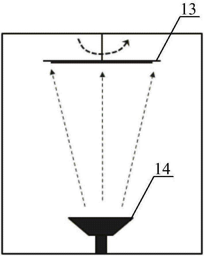
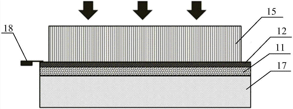
[0059] Such as Figure 1 ~ Figure 4 As shown, this embodiment provides a method for directly growing the scintillator layer of a flexible X-ray sensor. This method is a planar growth and packaging process, and is mainly applied to planar detectors and small-angle curved surface detectors. The growth method at least includes the following steps:

[0060] First, step 1-1) is performed to provide the flexible base layer 11 with the pixel array layer 12 prepared on the surface.

[0061] As an example, first provide a glass substrate 17, then coat the flexible substrate layer 11 on the surface of the glass substrate 17, and then grow the pixel array layer 12 on the surface of the flexible substrate layer 11, that is, from bottom to top These are the glass substrate 17 , the flexible substrate layer 11 , and the pixel array layer 12 in sequence.

[0062] It should be noted that the glass substrate 17 is mainly for the convenience of the planar growth process. The thickness of the ...

Embodiment 2

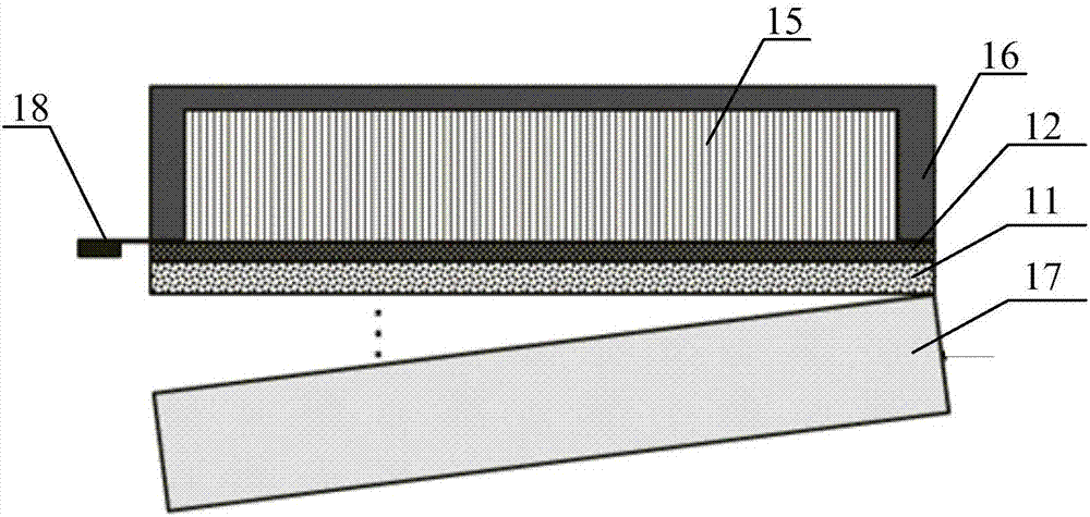
[0078] Such as Figure 8 ~ Figure 10 As shown, this embodiment provides a method for directly growing the scintillator layer of a flexible X-ray sensor. This method is a curved surface growth and packaging process, and is mainly applied to a curved surface detector with a large angle of curvature. The growth method at least includes the following steps:

[0079] First, step 2-1) is performed to provide the flexible base layer 21 with the pixel array layer 22 prepared on the surface.

[0080] As an example, first provide a glass substrate, then coat the flexible substrate layer 21 on the surface of the glass substrate, and then grow the pixel array layer 22 on the surface of the flexible substrate layer 21, that is, from bottom to top in order A glass substrate, a flexible substrate layer 21, and a pixel array layer 22.

[0081] The thickness of the glass substrate is 500-1000 μm. After the pixel array layer 22 is prepared and formed, the glass substrate needs to be separated f...


PUM

PropertyMeasurementUnit
Thicknessaaaaaaaaaa
Thicknessaaaaaaaaaa

Abstract

The invention provides a direct growth method of a flexible X-ray sensor scintillator layer. The growth method at least comprises the steps that firstly a flexible substrate layer of which the surfacehas preparation of a pixel array layer is provided; then the flexible substrate layer of which the surface has preparation of the pixel array layer is fixed on the plane support or the curved supportof the top part of a cavity, and a CsI scintillator layer is deposited on the surface of the pixel array layer by heating the CsI source of the bottom part of the cavity, wherein the CsI scintillatorlayer includes a CsI broken crystal layer and a CsI columnar crystal layer; and finally a sealed damp-proof layer is formed on the surface and the sidewall of the CsI scintillator layer. With application of the direct growth method, the CsI scintillator layer can be directly grown on the flexible substrate layer and the CsI layer can remain intact without crack when the sensor is bent, and the CsI can maintain performance without degradation even under the condition of multiple times of large-angle bending so as to have great reliability.

Description

technical field [0001] The invention relates to the technical field of flat panel detectors, in particular to a method for directly growing a scintillator layer of a flexible X-ray sensor. Background technique [0002] X-ray photography uses the short-wavelength and easy-to-penetrate nature of X-rays, and the different characteristics of X-ray absorption by different substances, and imaging by detecting the intensity of X-rays that pass through objects. As the core component of the X-ray imaging system, the flat panel detector (FPD: flat panel detector) is responsible for converting X-rays into electrical signals and recording images, which can be observed in due course through the display. [0003] In general, an FPD includes a scintillator, a pixel array, a control module, a signal processing module and a communication module. The scintillator absorbs X-rays and converts them into visible light; driven by the control module, the array absorbs the visible light generated b...

Claims


Application Information

Patent Timeline
IPC IPC(8): H01L27/146H01L31/0232G01T1/202
Inventor 欧阳纯方
Owner SHANGHAI IRAY TECH
Why Eureka
Try Eureka