Transparent and invisible RFID label material and preparation method
An RFID tag and invisible technology, applied in the field of RFID, can solve the problems of weak anti-bending ability, easy damage, loss of product authenticity and uniqueness of RFID tags, etc., achieve good anti-theft and anti-counterfeiting functions, reduce surface resistance, and have a wide range of applications Effect
- Summary
- Abstract
- Description
- Claims
- Application Information
AI Technical Summary
Problems solved by technology
Method used
Image
Examples
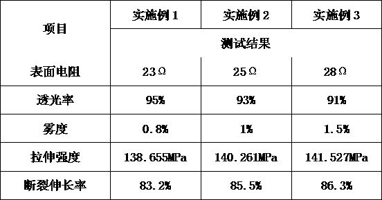
Embodiment 1
[0023] A kind of preparation of transparent invisible RFID tag material:
[0024] S1, take a PET film with a thickness of 0.01mm as the matrix film, lay it flat on the coating platform, and coat 0.1% nano-silver wire conductive silver paste on the matrix layer through a coating machine, the length and diameter of the nano-silver wire The ratio is 1000, the coating thickness is 30 μm, and the nano-silver wire conductive silver paste is cured at room temperature to obtain a conductive layer;
[0025] S2, preparation of conductive layer pattern: the conductive layer prepared in step S1 forms a conductive pattern by screen printing;
[0026] S3, preparation of the adhesive layer: the surface of the conductive layer prepared in step S2 is further coated with a UV-curable pressure-sensitive adhesive on the conductive layer, the coating thickness is 5 μm, and the thickness is 2 J / cm under the irradiation of a UV lamp. 2 The energy curing, that is, transparent invisible RFID label ma...
Embodiment 2
[0028] Preparation of a transparent invisible RFID label material:
[0029] S1, take a PE film with a thickness of 0.2mm as the matrix film, lay it flat on the coating platform, and coat 0.2% nano-silver wire and nano-silver particle conductive silver paste on the matrix layer through a coating machine, the nano-silver wire The ratio of length to diameter is 700, the coating thickness is 40 μm, and the conductive silver paste of nano-silver wire is cured at room temperature to obtain a conductive layer;
[0030] S2, preparation of conductive layer pattern: the conductive layer prepared in step S1 is mechanically embossed to form a conductive pattern;
[0031] S3, preparation of the adhesive layer: the surface of the conductive layer prepared in step S2 is further coated with a hot-melt adhesive on the conductive layer to a thickness of 8 μm, and cured at room temperature for 3 hours to obtain a transparent invisible RFID label material.
Embodiment 3
[0033] A kind of preparation of transparent invisible RFID tag material:
[0034] S1, take a PVC film with a thickness of 0.3mm as the matrix film, lay it flat on the coating platform, and coat 0.3% nano-silver wire conductive silver paste on the matrix layer through a coating machine, the length and diameter of the nano-silver wire The ratio is 500, the coating thickness is 50 μm, and the nano-silver wire conductive silver paste is cured at room temperature to obtain a conductive layer;
[0035] S2, preparation of conductive layer pattern: the conductive layer prepared in step S1 is mechanically embossed to form a conductive pattern;
[0036] S3, preparation of the adhesive layer: the surface of the conductive layer prepared in step S2 is further coated with a solvent-based resin adhesive on the conductive layer to a thickness of 10 μm, and cured at room temperature for 3 hours to obtain a transparent invisible RFID label material.
[0037] The production of conductive lines...
PUM
| Property | Measurement | Unit |
|---|---|---|
| thickness | aaaaa | aaaaa |
| thickness | aaaaa | aaaaa |
| thickness | aaaaa | aaaaa |
Abstract
Description
Claims
Application Information
