Method and system for noise mitigation in multi-beam scanning electron microscopy system

An electron microscope, electron microscope technology, applied in microscopes, circuits, discharge tubes, etc., can solve problems such as shortening inspection time, separation of noise and image information, and lack of sufficient feature information to extract noise.

Active Publication Date: 2018-05-11
KLA TENCOR CORP
View PDF5 Cites 5 Cited by
  • Summary
  • Abstract
  • Description
  • Claims
  • Application Information

AI Technical Summary

Problems solved by technology

In single-beam SEM systems, it is often difficult to separate noise from image information
This difficulty arises from the fact that: i) it is difficult to determine that image artifacts are noise and not actual image features; and ii) there may not be enough characteristic information in a single image

Method used


Image

  • Method and system for noise mitigation in multi-beam scanning electron microscopy system
  • Method and system for noise mitigation in multi-beam scanning electron microscopy system
  • Method and system for noise mitigation in multi-beam scanning electron microscopy system

Examples


Embodiment Construction

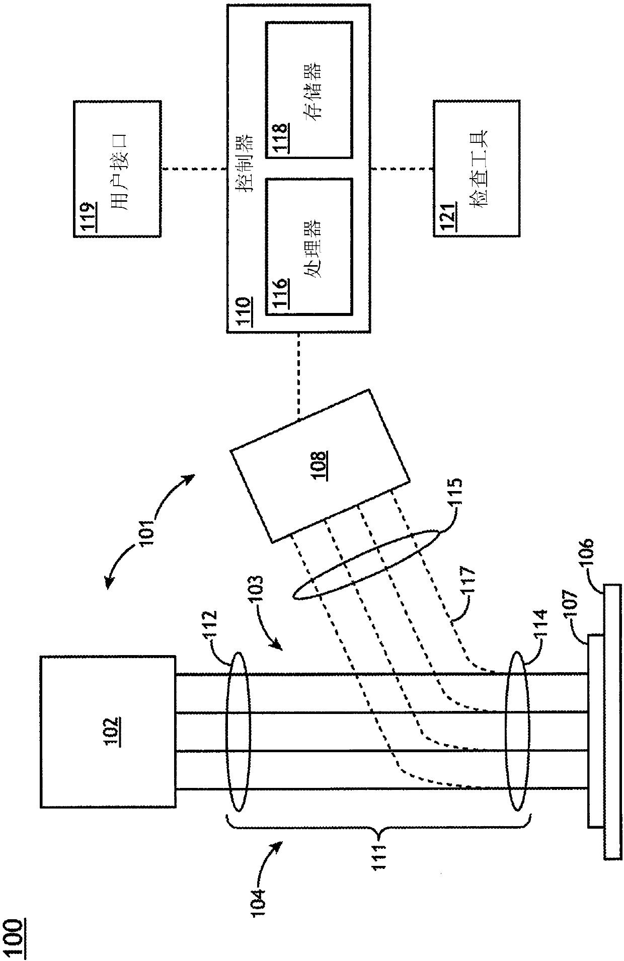
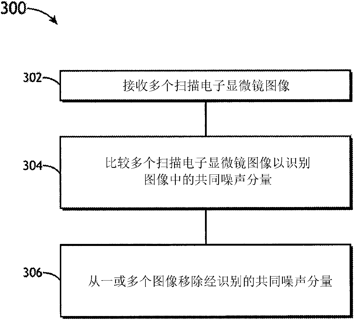
[0018] Reference will now be made in detail to the disclosed subject matter which is illustrated in the accompanying drawings. generally refer to figure 1 A to 3C, systems and methods for reducing noise in a multi-beam scanning electron microscope (SEM) imaging system are described according to the present invention.

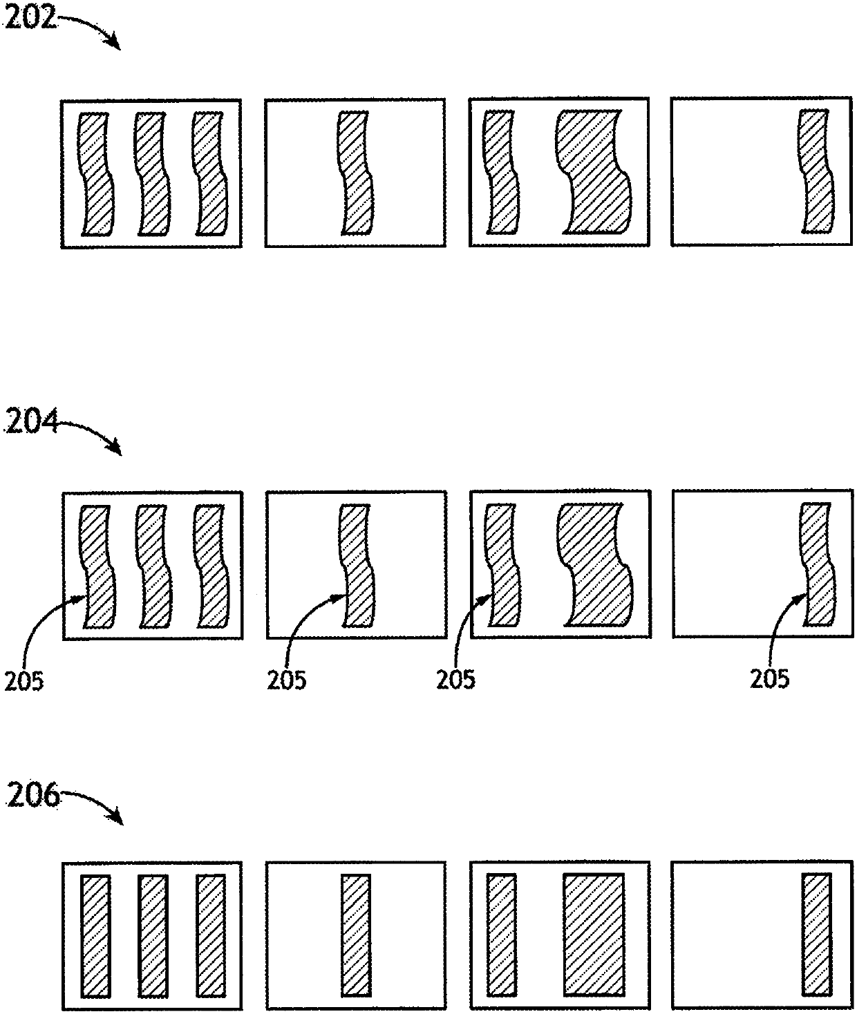
[0019] Embodiments of the invention relate to reducing or eliminating common mode noise in multi-beam SEM systems. It should be noted that this noise can come from a variety of sources including, but not limited to, vibrational noise, acoustic noise, electrical noise (eg, 60Hz noise), errors / faults in the high voltage power supply, and intensity noise occurring in the electron source or electron gun. Noise components may be positional noise (eg, at x-position, y-position, and / or z-position (focus)) or intensity (ie, brightness). Additional embodiments of the invention relate to correcting for the presence of noise components in multiple images (eg via image p...


PUM


Abstract

A scanning electron microscopy system is disclosed. The system includes a multi-beam scanning electron microscopy (SEM) sub-system. The SEM sub-system includes a multi-beam electron beam source configured to generate a plurality of electron beams, a sample stage configured to secure a sample, an electron-optical assembly, and a detector assembly configured to detect a plurality of electron signalbeams emanating from the surface of the sample to form a plurality of images, each image associated with an electron beam of the plurality of electron beams. The system includes a controller configured to receive the images from the detector assembly, compare two or more of the images to identify common noise components present in the two or more images, and remove the identified common noise components from one or more images of the plurality of images.

Description

[0001] Cross References to Related Applications [0002] The inventors claimed in this application under 35 U.S.C. §119(e) are Mark McCord, Rainer Knippelmeyer, Douglas Masnaghetti, and Richard Simon ( Richard Simmonrs, U.S. Provisional Application Serial No. 62 / 221,599, filed September 21, 2015, entitled "TECHNIQUEFOR NOISE REJECTION IN A MULTIPLE-BEAM IMAGING SYSTEM" and constitutes a formal (non-provisional) patent application to said U.S. Provisional Application, which is hereby incorporated by reference in its entirety. technical field [0003] The present invention relates generally to scanning electron microscopy, and more particularly to noise reduction in multi-beam electron microscopy systems. Background technique [0004] The fabrication of semiconductor devices, such as logic and memory devices, typically involves processing a substrate, such as a semiconductor wafer, using a number of semiconductor fabrication processes to form various features and multiple le...

Claims


Application Information

Patent Timeline
IPC IPC(8): G02B21/22G02B21/00
CPCH01J37/09H01J2237/0216H01J2237/2817H01J37/222H01J37/28G02B21/22G02B21/0032G02B21/008
Inventor M·A·麦科德R·克尼彭迈耶D·马斯纳盖蒂R·R·西蒙斯
Owner KLA TENCOR CORP
Why Eureka
Try Eureka