Miniature spectral imaging system and imaging method

An imaging system and spectral imaging technology, which is applied in spectrum investigation and other fields, can solve the problem of reducing spatial resolution and achieve the effects of high system integration, low cost, and low power consumption

Active Publication Date: 2018-05-22
CHANGCHUN INST OF OPTICS FINE MECHANICS & PHYSICS CHINESE ACAD OF SCI
View PDF3 Cites 6 Cited by
  • Summary
  • Abstract
  • Description
  • Claims
  • Application Information

AI Technical Summary

Problems solved by technology

[0004] The present invention provides a miniaturized spectral imaging system and imaging method to solve the problem of improving the signal-to-noise ratio and reducing the spatial resolution of the target in the existing CMOS hyperspectral imaging technology

Method used


Image

  • Miniature spectral imaging system and imaging method
  • Miniature spectral imaging system and imaging method
  • Miniature spectral imaging system and imaging method

Examples


specific Embodiment approach 1

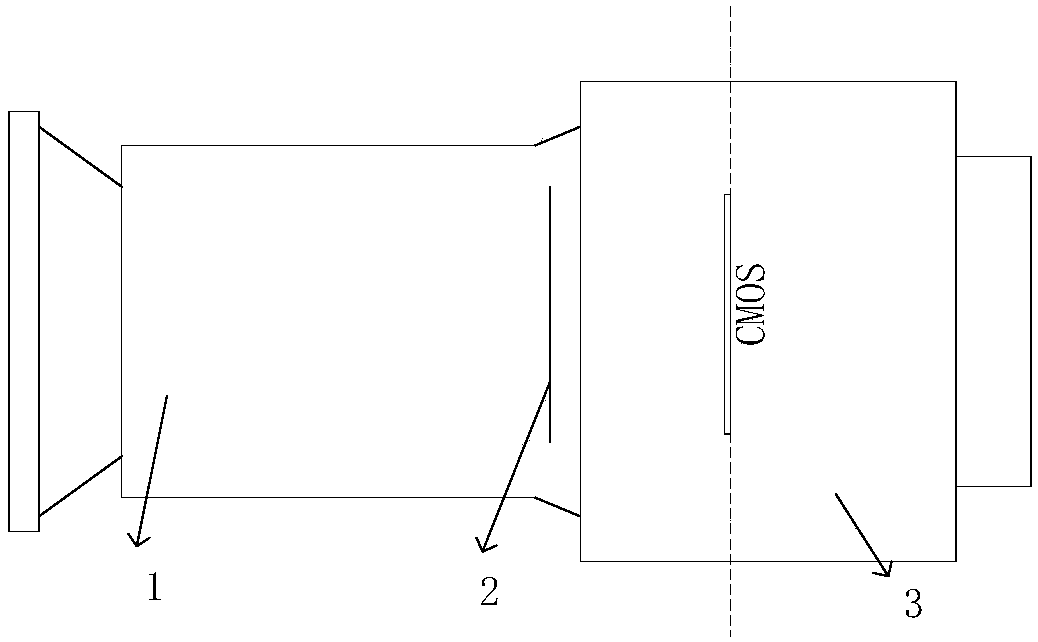
[0035] Specific implementation mode 1. Combination Figure 1 to Figure 3 Describe this embodiment, a miniaturized high-sensitivity high-resolution hyperspectral imaging system, including a lens 1 , a spectroscopic element 2 , and imaging system electronics 3 . After the lens 1 collects the incident light, it focuses and projects it to the spectroscopic element 2. After passing through the spectroscopic element 2, the light is subdivided into the required n narrow bands. The imaging system electronics 3 receives the n spectral bands of light and converts them into electric signal.

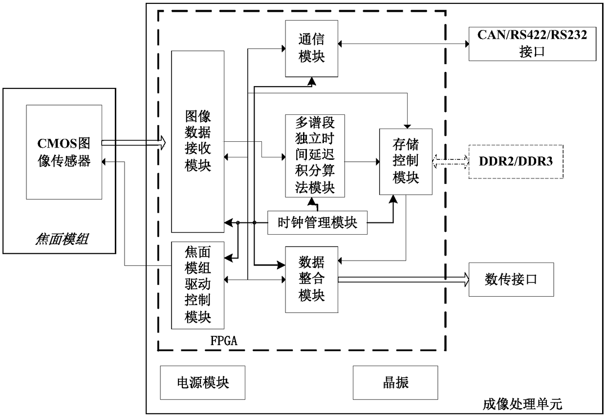
[0036] The lens described in this embodiment can use conventional components, and the light splitting element can use filters, prisms, gratings, interference light splitting, etc., and both the lens and the light splitting element can use mature products. The imaging system electronics includes a focal plane module and an imaging processing unit, which are the key protection parts of this patent. ...

specific Embodiment approach 2

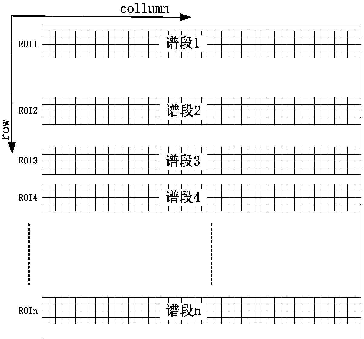
[0039] Specific embodiment two, combine Figure 4 Describe this embodiment. This embodiment is an imaging method for a miniaturized, high-sensitivity, and high-resolution hyperspectral imaging system described in Embodiment 1. The imaging method is divided into two processes, namely the spectral position fast calibration mode and high Spectral imaging mode. The calibration mode is used to quickly calibrate the projection positions of n wavelength spectra on the focal plane of the sensor after the imaging system is assembled. After the calibration is completed, the imaging system can carry out formal hyperspectral imaging according to the calibration results. Such as Figure 4 shown.

[0040] The technical scheme adopted in the spectral position rapid calibration mode is as follows:

[0041] Step 1: Set the imaging mode to the spectral position quick calibration mode;

[0042] Step 2: The programmable logic device generates the sensor drive control timing in the calibration...


PUM


Abstract

The invention relates to a miniature spectral imaging system and imaging method, and relates to the technical field of photoelectric imaging, solving the problems that in the current high spectral imaging technology of CMOS, the spatial resolution of the target is reduced when the signal to noise ratio is improved. The miniature spectral imaging system includes a lens, a beam splitting element andimaging system electronics, wherein the incident light is projected to the beam splitting element through focusing of the lens, and after the incident light passes by the beam splitting element, theincident light is divided into n narrow spectral bands; and the imaging system electronics can receive the light from the n spectral bands and convert the light into electric signals. The imaging method includes two processes: quick calibration of spectrum position and high spectral imaging. The calibration process is used for quickly calibrating the projection positions of the n wave length spectrums on the focal plane of the sensor after assembling of the imaging system is completed, and then the imaging system performs high spectral imaging according to the calibration result after calibration is over. The miniature spectral imaging system and imaging method use the CMOS image sensor with a function of opening multiple windows in the row direction, thus being low in power consumption, being low in cost and being high in the system integration level so as to satisfy the demand for light and miniaturization development of high spectral imaging.

Description

technical field [0001] The invention relates to the technical field of photoelectric imaging, in particular to a miniaturized spectral imaging system and an imaging method. Background technique [0002] Spectral imaging technology can obtain the spectral information of the target while obtaining the two-dimensional spatial feature information of the target. Therefore, it has a broad application space and plays an important role in the fields of military reconnaissance, agricultural and forestry observation, environmental monitoring, disaster investigation, and geological exploration. . Among them, hyperspectral imaging systems play an important role in most fields of natural science and some fields of people's lives, such as crop yield estimation, soil quality assessment, water pollution detection, air pollution detection, etc. However, at present, most domestic hyperspectral imaging systems have the problems of large volume and weight, high power consumption, high cost, an...

Claims


Application Information

Patent Timeline
Patent Type & Authority Applications(China)
IPC IPC(8): G01J3/28
Inventor 陶淑苹张续严金光徐伟曲宏松吴勇
Owner CHANGCHUN INST OF OPTICS FINE MECHANICS & PHYSICS CHINESE ACAD OF SCI
Why Eureka
Try Eureka