Heterostructures and electronic devices derived therefrom

一种异质结、叠层结构的技术,应用在电气元件、半导体器件、电路等方向,能够解决电荷不均匀性降低、石墨烯电子迁移率增加等问题

Inactive Publication Date: 2018-05-22
NANOCO 2D MATERIALS LTD
View PDF1 Cites 7 Cited by
  • Summary
  • Abstract
  • Description
  • Claims
  • Application Information

AI Technical Summary

Problems solved by technology

This is manifested in increased electron mobility and reduced charge inhomogeneity in graphene

Method used


Image

  • Heterostructures and electronic devices derived therefrom
  • Heterostructures and electronic devices derived therefrom
  • Heterostructures and electronic devices derived therefrom

Examples


Embodiment Construction

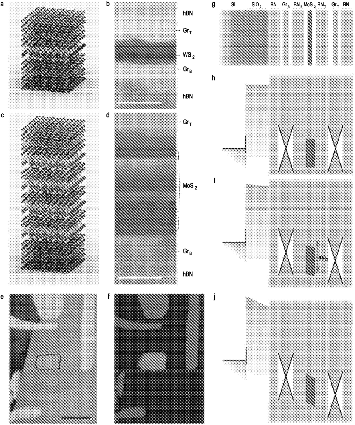
[0134] The term "vertical heterojunction" refers to multiple two-dimensional crystals arranged in a stack. A heterojunction includes at least two different materials. The two-dimensional crystals are arranged such that the heterojunctions are substantially parallel, arranged face-to-face, forming a stack. Such a heterojunction may also be referred to as a two-dimensional heterojunction.

[0135] For the purposes of the present invention, heterojunctions are formed entirely of two-dimensional crystals. This does not exclude that the heterojunction is mounted on a substrate and / or has a protective coating. A two-dimensional heterojunction is what is called a two-dimensional heterojunction because it is composed of two-dimensional crystals. Of course, it will itself be a three-dimensional structure.

[0136] Examples of two-dimensional crystals that can be included in the heterojunction of the present invention include: graphene, modified graphene (for example, doped graphene...


PUM

PropertyMeasurementUnit
draft ratioaaaaaaaaaa

Abstract

The advent of graphene and related 2D materials has recently led to a new technology: heterostructures based on these atomically thin crystals. The paradigm proved itself extremely versatile and led to rapid demonstration of tunnelling diodes with negative differential resistance, tunnelling transistors, photovoltaic devices and so on. In the present invention, the complexity and functionality ofsuch van der Waals heterostructures is taken to the next level by introducing quantum wells (QWs) engineered with one atomic plane precision. We describe light-emitting diodes (LEDs) made by stackingmetallic graphene, insulating hexagonal boron nitride and various semiconducting monolayers into complex but carefully designed sequences.

Description

technical field [0001] The advent of graphene and related 2D materials has recently led to a new technology: heterojunctions based on these atomically thick crystals. The paradigm proved itself to be very diverse and resulted in rapid demonstrations of tunnel diodes, tunnel transistors, photovoltaics, etc. with negative differential resistance. [0002] In the present invention, the complexity and functionality of such van der Waals heterojunctions is taken to the next level by introducing quantum wells (QWs) designed with one atomic plane precision. This paper describes light-emitting diodes (LEDs) fabricated by stacking metallic graphene, insulating hexagonal boron nitride, and various semiconductor monolayers in a complex but well-designed sequence. [0003] Accordingly, the present invention relates to vertical heterojunctions and devices derived from such structures, such as light emitting diodes (LEDs). Specifically, a heterojunction includes a stacked structure compri...

Claims


Application Information

Patent Timeline
Patent Type & Authority Applications(China)
IPC IPC(8): H01L33/06H01L33/26H01L33/32H01L33/34H01L29/15H01L29/16H01L29/24H01L29/267H01L29/41H05B33/14H05B33/20H05B33/26
CPCH01L29/267H01L29/1606H01L29/24H05B33/145H05B33/20H05B33/26H01L29/413H01L33/06H01L33/26H01L33/32H01L33/34H01L29/152
Inventor 弗雷德里克·威特斯康斯坦丁·诺沃肖洛夫
Owner NANOCO 2D MATERIALS LTD
Why Eureka
Try Eureka