Tunneling gap diodes

Inactive Publication Date: 2006-08-17
BOREALIS TECH LTD
View PDF8 Cites 17 Cited by
  • Summary
  • Abstract
  • Description
  • Claims
  • Application Information

AI Technical Summary

Benefits of technology

[0010] The present invention discloses a tunneling diode having a band gap material as the collector, or having a metal electrode coated by a film of band gap material with a thickness greater than the mean distance of relaxation of tunneled emitter electrons (˜10 nm or more). This increases the tunneling of electrons having greater energy than the Fermi level from emitter to collector, leading to an increase in the efficiency of heat pumping or power generation by the diode. In the context of this invention, the term “band gap material” is defined as a crystal material having a filled zer

Problems solved by technology

However, for room temperature cooling effects, materials having work functions of the order of ˜0.3-0.35 eV are needed for the emitter, and such materials are not practically available.
As a result, high cooling power up to 10 W/cm2 and more may be obtained, but at very low efficiency (˜1% or less) Thus appro

Method used


Image

  • Tunneling gap diodes
  • Tunneling gap diodes
  • Tunneling gap diodes

Examples


example 1

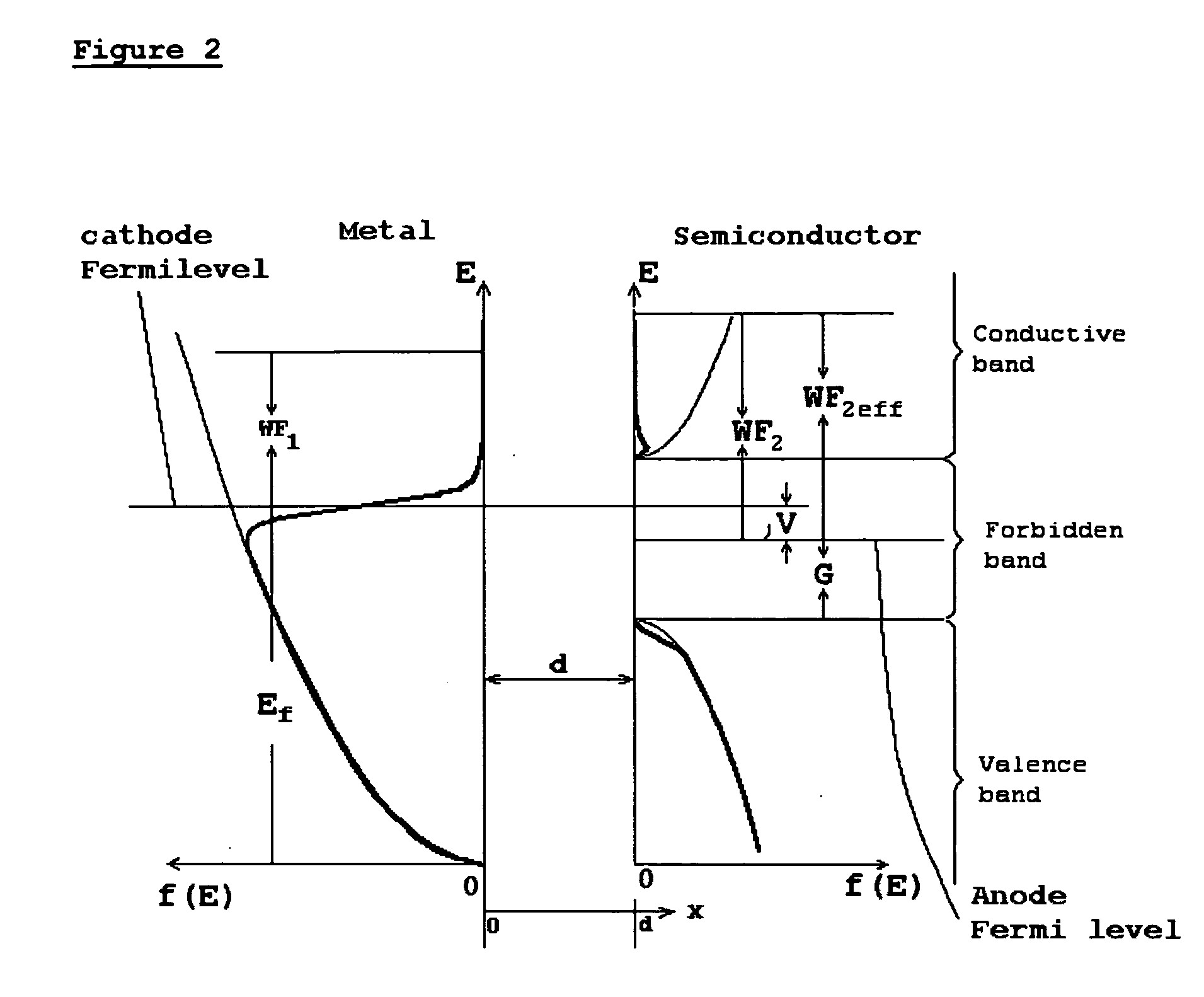
[0040] In one embodiment, pure Ge is the semiconductor. It has G=0.75 eV, and G / 2=0.375 eV, a little more than optimum WF for thermionic diode for Tc (temperature of emitter, cold electrode, hereafter referred to as T1)=300K (”0.33eV). Even at room temperature, Ge has electron concentration in conductive band ˜1013 cm−3, which is sufficient for electrical conductivity for thin layer. If it is assumed that electrodes are treated by Cs and O2 and has WF1=WF2=1 eV, then the output parameters for cooling with d=2.5 nm, T1=300K, Th (temperature of collector, hot electrode, hereafter referred to as T2)=350K are given below:

hcool / hcoolV, Vj, A / cm2Qc, W / cm2W, W / cm2COPhcoolCarnot0.101.760.630.1773.560.780.910.146.822.220.7962.320.6990.8160.2036.69.707.3151.320.570.665

[0041] Here j is resulting diode current, Qc cooling power, W=j*V=spent power. Calculations were fulfilled with some simplifications as follows.

[0042] For elementary tunnel current from emitter, which is produced by electrons...

example 2

[0057] In a further embodiment, the tunnel diodes of the present invention are workable in the low (cryogenic) temperature region with relatively high efficiency, if the distance between Fermi level and the bottom of the conductive band (E0) of the collector is sufficiently low.

[0058] Referring to FIG. 4, the dependence of two main parameters of cooled device, namely cool power Q and relation of cooling efficiency h to Carnot efficiency hc, are shown in relation to the bias at various values of parameter G (energy difference between an anode Fermi level and a bottom of conductive band of semiconductor). Regime is: d=2.5 nm (all calculations have done for this gap, the currents are not too big for it), T1=20K (liquid H2), T2=40K. G values are: 1-0.007 ev, 2-0.01, 3-0.02, 4-0.03, 5-0.04, 6-0.05. The green line is the cool power, and the red line is h / hc. It is seen firstly, that parameters are more than good in spite of such a low T1. Note, for common metal—metal case cooling is stop...


PUM


Abstract

The present invention discloses a tunneling diode having a band gap material as the collector. This increases the tunneling of electrons having greater energy than the Fermi level from emitter to collector, leading to an increase in the efficiency of heat pumping or power generation by the diode. In a further embodiment the collector comprises a semiconductor on which a layer of band gap material is deposited. This approach also reduces back tunneling of electrons from collector to emitter.

Description

CROSS-REFERENCE TO RELATED APPLICATIONS [0001] This application is a Continuation in Part of patent application Ser. No. ______ (application number not yet known) filed Mar. 22, 2006, which is the U.S. national stage application of International Application PCT / US04 / 031221, filed Sep. 22, 2004, which international application was published on Apr. 7, 2005, as International Publication WO2005 / 031780 in the English language. The International Application claims the benefit of U.K. Application No. GB0322116.5, filed Sep. 22, 2003. This application also claims the benefit of U.S. Provisional Application No. 60 / 666,654, filed Mar. 29, 2005.BACKGROUND OF THE INVENTION [0002] This invention relates to tunneling diodes and their application to heat pumping and power generation. [0003]“Cool Chip” is hereby defined as a device that uses electrical power or energy to pump heat, thereby creating, maintaining, or degrading a thermal gradient. Cool Chips may accomplish this using thermionics, the...

Claims


Application Information

Patent Timeline
IPC IPC(8): H01L29/88H01L21/331
CPCH01J21/04H01L29/88
Inventor MARTSINOVSKY, ARTEMI MARKOVICH
Owner BOREALIS TECH LTD
Why Eureka
Try Eureka