Si/SiGe interband tunneling diode structures including SiGe diffusion barriers

a tunneling diode and interband technology, applied in the field ofsemiconductor arts, can solve the problems of difficult production of the structure of the tunneling diode and limited thermal budget, and achieve the effect of suppressing the diffusion of acceptors

Inactive Publication Date: 2007-11-20
THE UNITED STATES OF AMERICA AS REPRESENTED BY THE SECRETARY OF THE NAVY +1
View PDF3 Cites 12 Cited by
  • Summary
  • Abstract
  • Description
  • Claims
  • Application Information

AI Technical Summary

Benefits of technology

[0009]According to one aspect, a silicon-based interband tunneling diode includes a degenerate p-type doping of acceptors, a degenerate n-type doping of donors disposed on a first side of the degenerate p-type doping, and a barrier silicon-ger

Problems solved by technology

The ITD structure is challenging to produce, because dopant segregation and dopant diffusion during growth lowers the doping density and degrades the negative differential resistance (NDR).
However, low temperature epitaxy also typically introduces higher point defect concentrations w

Method used


Image

  • Si/SiGe interband tunneling diode structures including SiGe diffusion barriers
  • Si/SiGe interband tunneling diode structures including SiGe diffusion barriers
  • Si/SiGe interband tunneling diode structures including SiGe diffusion barriers

Examples


Embodiment Construction

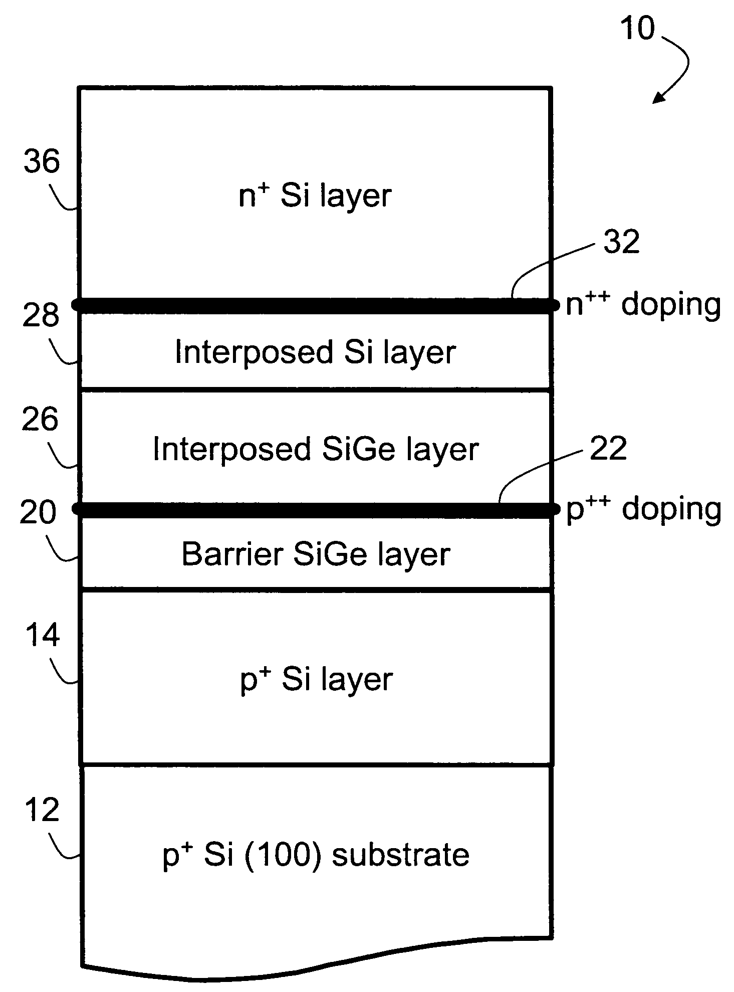
[0021]With reference to FIG. 1, an example interband tunneling diode (ITD) 10 is formed on a p+ silicon substrate 12. The ITD 10 includes a plurality of group IV layers epitaxially grown on the substrate 12 by a suitable low temperature epitaxy method that reduces dopant segregation and diffusion during epitaxial growth, such as low temperature molecular beam epitaxy (LT-MBE), low pressure chemical vapor deposition (LPCVD), ultra-high vacuum chemical vapor deposition (UHV-CVD), solid phase epitaxy, or the like. In the illustrated example embodiment, the ITD 10 includes an epitaxial p+ silicon layer 14 grown on the substrate 12 and a barrier silicon-germanium layer 20 grown on the p+ silicon layer 14, followed by formation of a degenerately p-type doped region 22. In FIG. 1, the degenerately doped p-type region 22 is a p-type delta doping formed as follows: during a growth interruption in which the group IV epitaxial growth is interrupted, an acceptor species is applied to the expose...


PUM


Abstract

A silicon-based interband tunneling diode (10, 110) includes a degenerate p-type doping (22, 130) of acceptors, a degenerate n-type doping (32, 118) of donors disposed on a first side of the degenerate p-type doping (22, 130), and a barrier silicon-germanium layer (20, 136) disposed on a second side of the degenerate p-type doping (22, 130) opposite the first side. The barrier silicon-germanium layer (20, 136) suppresses diffusion of acceptors away from a p/n junction defined by the degenerate p-type and n-type dopings (22, 32, 118, 130).

Description

[0001]This application claims the benefit of U.S. Provisional Application Ser. No. 60 / 492,039 filed on Aug. 1, 2003. This application is a continuation-in-part application of U.S. application Ser. No. 09 / 934,334 filed Aug. 21, 2001, which is a divisional application of U.S. application Ser. No. 09 / 565,455 filed May 5, 2000 which issued as U.S. Pat. No. 6,803,598 on Oct. 12, 2004, which claims the benefit of U.S. Provisional Application Ser. No. 60 / 133,067 filed May 7, 1999.[0002]U.S. Provisional Application Ser. No. 60 / 492,039 is incorporated by reference herein in its entirety. U.S. patent application Ser. No. 09 / 934,334, filed on Aug. 21, 2001 and published as US 2003-0049894 A1 on Mar. 13, 2003, is incorporated by reference herein in its entirety.[0003]This invention was made with Government support under grant no. ECS-0196208 awarded by the National Science Foundation and under grant no. ECS-196054 awarded by the National Science Foundation. The Government has certain rights in ...

Claims


Application Information

Patent Timeline
IPC IPC(8): H01L29/00
CPCH01L29/885
Inventor BERGER, PAUL R.THOMPSON, PHILLIP E.JIN, NIU
Owner THE UNITED STATES OF AMERICA AS REPRESENTED BY THE SECRETARY OF THE NAVY
Why Eureka
Try Eureka