Nanotunneling junction-based hyperspectral polarimetric photodetector and detection method

a hyperspectral polarimetric and photodetector technology, applied in the field of photodetectors, can solve the problems of limited application, low detectivity, slow response time, etc., and achieve the effect of high signal-to-noise ratio

Inactive Publication Date: 2009-03-10
NAT AERONAUTICS & SPACE ADMINISTATION U S GOVERNMENT AS REPRESENTED BY THE ADMINISTATOR OF THE
View PDF14 Cites 16 Cited by
  • Summary
  • Abstract
  • Description
  • Claims
  • Application Information

AI Technical Summary

Problems solved by technology

While these thermal detectors can be operated at room temperature, they present several drawbacks, particularly, low detectivity and slow response time, which limits their applications.
The requirement of cryo-cooling makes semiconductor-based photon detectors bulky, heavy, expensive, dependent on additional power supplies, and impractical for many applications.
Unfortunately, to date the performance of uncooled and room temperature sensors has been inferior to that of cooled sensors.
This performance gap limits the number of applications and precludes the widespread use of uncooled infrared sensors in most photon (including IR) sensor applications.
But thermal FPAs suffer from low detectivity (108-109 cmHz½ / W) and slow response time (tens of msec).
The same issues arise with narrowband detectors like quantum-well-intersubband-photon detectors (QWIP).
However, this and other known systems operating in a one-dimensional scanned mode are complex with moving optical filters, and often are power-hungry.
Furthermore, current state-of-the-art FPAs are limited to no more than 4 colors, using either HgCdTe or quantum well infrared photodetectors (QWIP).
The vertical integration of wavelength-selective QWIPs or HgCdTe detectors in a 3D cube configuration have an inherent limitation due to severe challenges in material growth, spectral resolution at each pixel, and read-out circuitry / power dissipation.
In sum, none of the current state-of-the-art imagers / FPAs offers the functionality of simultaneous multispectral and polarimetric sensing, and the conventional IR detection approaches that they rely on fail to achieve the necessary performance metrics.

Method used


Image

  • Nanotunneling junction-based hyperspectral polarimetric photodetector and detection method
  • Nanotunneling junction-based hyperspectral polarimetric photodetector and detection method
  • Nanotunneling junction-based hyperspectral polarimetric photodetector and detection method

Examples


Embodiment Construction

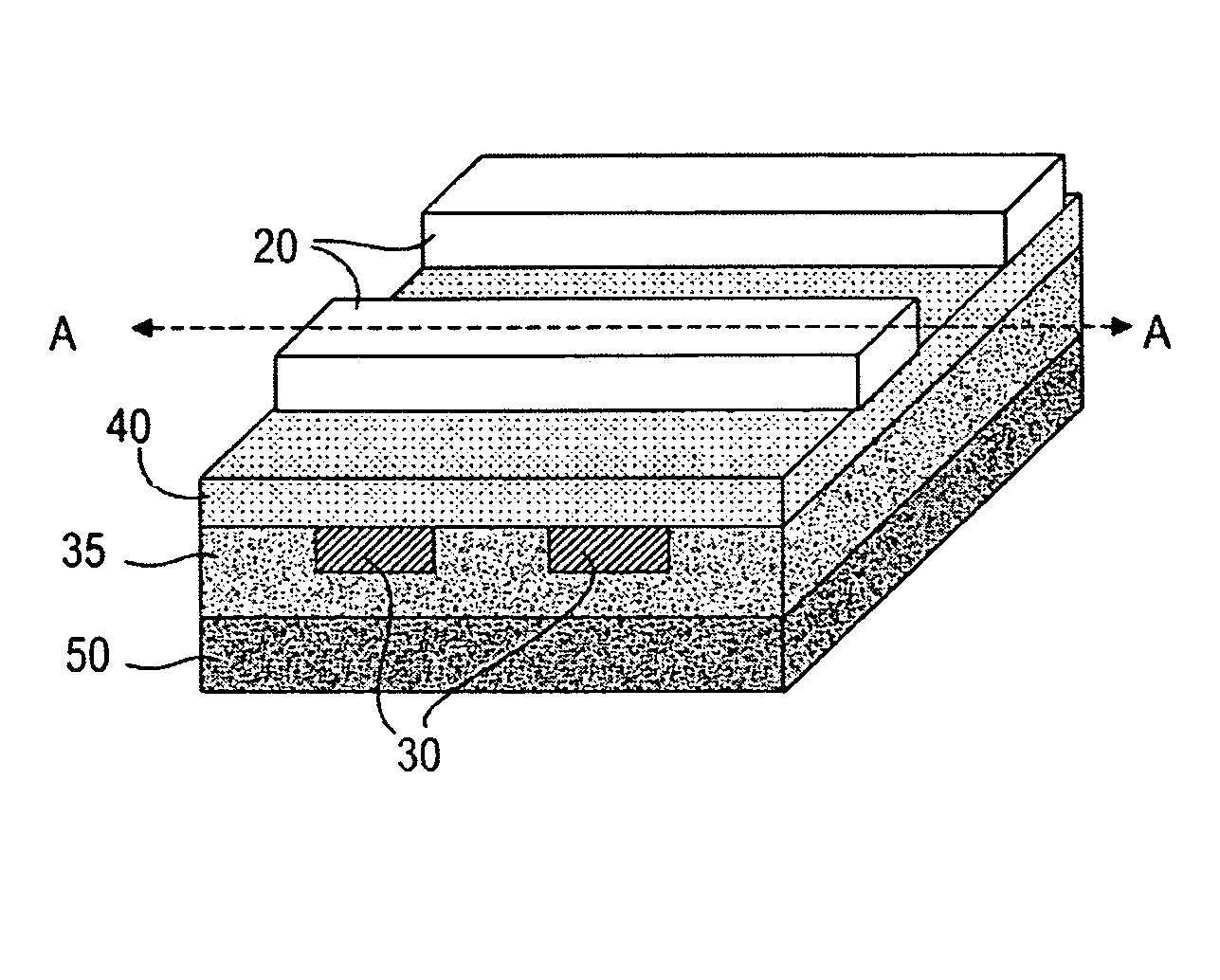
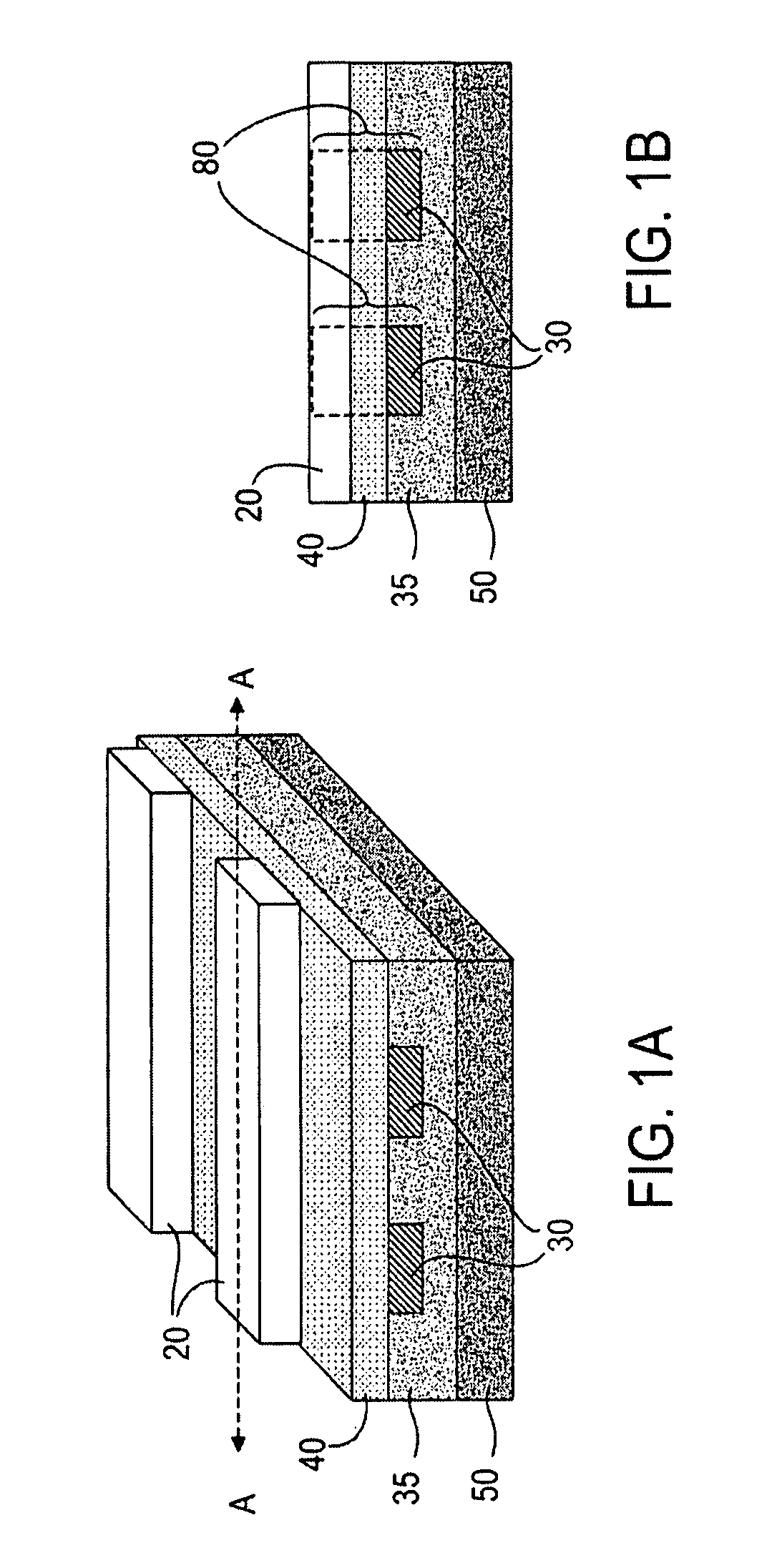
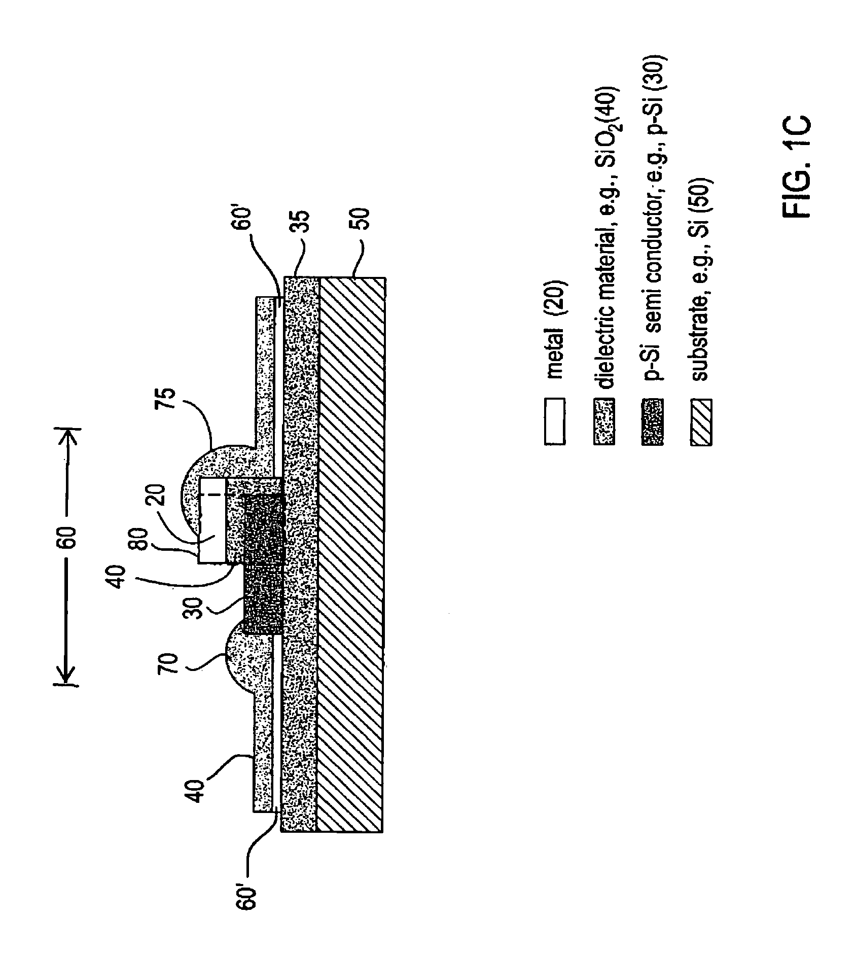
[0029]The present invention is an antenna-coupled nanojunction photodetector and method of operation that senses tunneling current at a nanometer-scale tunneling junction (NTJ), rather than by conventional thermal or photon means. The nanojunction consist of a mesh of crossing nanowires and therefore lends itself to micro / nano fabrication techniques. Indeed, a large format array of nano-tunneling-junction-based detector can be formed on single FPA chip to provide the capability of simultaneous hyperspectral and polarimetric sensing within a spectral band. Moreover, the array enables uncooled, and low power multi-spectral imaging with a fast frame rate and temporal response, high directivity and high spatial resolution.

[0030]FIG. 1A is a perspective view of a nano junction photodetector array 2 comprising an exemplary set of four (4) nano tunnelinging junctions (NTJs) 80 with two stacks of nanowire arrays 20, 30 in a crossbar geometry interfaced with an ultra thin dielectric layer 40...


PUM


Abstract

A photodetector, detector array, and method of operation thereof in which nanojunctions are formed by crossing layers of nanowires. The crossing nanowires are separated by a few nm thick electrical barrier layer which allows tunneling. Each nanojunction is coupled to a slot antenna for efficient and frequency-selective coupling to photo signals. The nanojunctions formed at the intersection of the crossing wires defines a vertical tunneling diode that rectifies the AC signal from a coupled antenna and generates a DC signal suitable for reforming a video image. The nanojunction sensor allows multi/hyper spectral imaging of radiation within a spectral band ranging from terahertz to visible light, and including infrared (IR) radiation. This new detection approach also offers unprecedented speed, sensitivity and fidelity at room temperature.

Description

STATEMENT OF GOVERNMENT INTEREST[0001]The invention described hereunder was made in the performance of work under a NASA contract, and is subject to the provisions of Public Law #96-517 (35 U.S.C. 202) in which the Contractor has elected not to retain title.BACKGROUND OF THE INVENTION[0002]1. Field of the Invention[0003]The present invention generally relates to photodetectors and, more particularly, to a photodetector that detects radiation within a spectral band ranging from terahertz to visible light, including infrared (IR) radiation. The disclosed detector comprises a high density nano-tunneling-junction-based photodetector array, rather than by conventional thermal or photodetectors. This detection mechanism improves response time and sensitivity, and avoids the need for cooling to cut thermal noise.[0004]2. Description of Prior Art[0005]A focal plane array (FPA) is a matrix of detector cells attached to a semiconductor chip. The detector cells absorb IR radiation, convert it ...

Claims


Application Information

Patent Timeline
Patent Type & Authority Patents(United States)
IPC IPC(8): G01T1/24
CPCG01J5/02G01J5/023G01J5/08G01J5/0837G01J5/10H04N5/33
Inventor SON, KYUNG-AHMOON, JEONGSUN J.CHATTOPADHYAY, GOUTAMLIAO, ANNATING, DAVID
Owner NAT AERONAUTICS & SPACE ADMINISTATION U S GOVERNMENT AS REPRESENTED BY THE ADMINISTATOR OF THE
Why Eureka
Try Eureka