Oscillation device and inspection apparatus

a technology of oscillation device and inspection apparatus, which is applied in the direction of oscillation generator, semiconductor device, pulse technique, etc., can solve the problems of single device not being able to produce frequencies that differ to a large extent, and the device cannot accommodate a plurality of spectrums, so as to reduce the number of oscillation devices employed, the effect of low power consumption

Active Publication Date: 2009-02-26
CANON KK
View PDF4 Cites 15 Cited by
  • Summary
  • Abstract
  • Description
  • Claims
  • Application Information

AI Technical Summary

Benefits of technology

[0018]The oscillation wavelength can effectively be shifted when the thickness adjusting layers are within a range not less than 5 nm and not more than 60 nm.
[0021]The present invention can provide a compact and low power consumption system including a sensor apparatus or an imaging apparatus that operates in the terahertz region as described in the Related Art section by using an oscillation device according to the present invention.
[0022]Thus, a single oscillation device according to the present invention can oscillate in two frequencies. When an inspection apparatus for inspecting the presence or absence of a specific substance by means of the fingerprint spectrum thereof is formed by using oscillation devices according to the present invention, the number of oscillation devices that are employed can be reduced if compared ordinary arrangements where a considerable number of oscillation devices that correspond to various spectrums are required.

Problems solved by technology

Generally, the oscillation frequency cannot be changed to a large extent in such semiconductor oscillation devices in the terahertz wave region so that a large number of oscillation devices having different oscillation frequencies need to be prepared in order to apply such devices to inspections for identifying a substance by means of a fingerprint spectrum in the inside of the substance.
However, the change in the oscillation frequency is slight and about several % at most so that such a device cannot accommodate a plurality of spectrums.
Therefore, as well known, while the Q value of the resonator is relatively large and the oscillation frequency changes as the equivalent permittivity of the entire inside changes, a single device cannot produce frequencies that differ to a large extent.

Method used


Image

  • Oscillation device and inspection apparatus
  • Oscillation device and inspection apparatus
  • Oscillation device and inspection apparatus

Examples


example 1

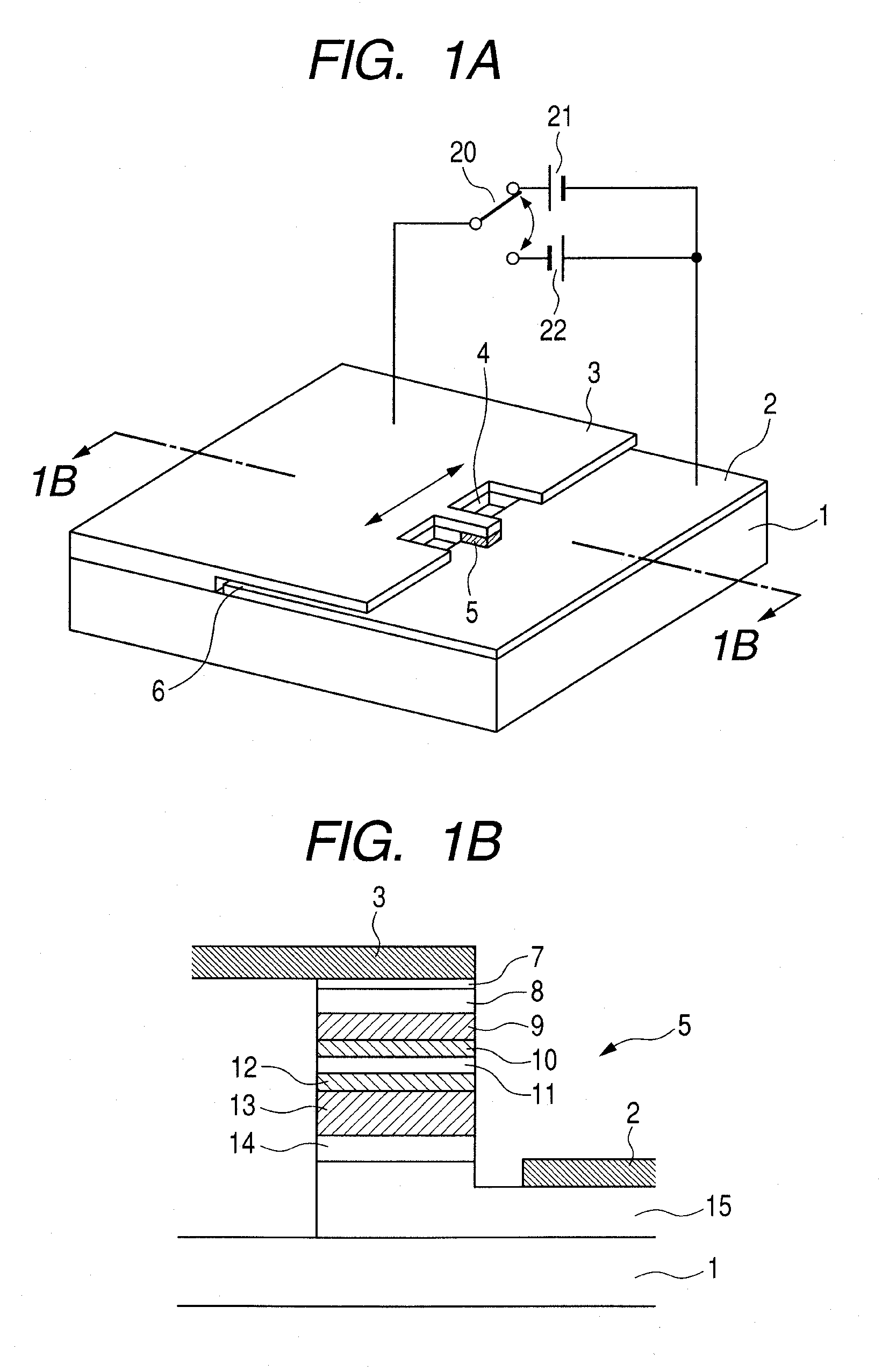
[0060]The first example of the present invention is an oscillation device having a structure as illustrated in FIGS. 1A and 1B with an antenna length of 50 μm and a semiconductor layer 5 forming a resonant tunneling diode and illustrating a post-shaped profile with a width of 2.5 μm. The semiconductor layers forming the device have the respective thicknesses as listed below:[0061]n+-InGaAs contact layer 15: 400 nm;[0062]n-InGaAs layer 14: 50 nm;[0063]first non-doped InGaAs thickness adjusting layer 13: 40 nm;[0064]first non-doped AlAs barrier layer (In=0) 12: 1.5 nm;[0065]non-doped InGaAs quantum well layer 11: 4.5 nm;[0066]second non-doped AlAs barrier layer (In=0) 10: 1.5 nm;[0067]second non-doped InGaAs thickness adjusting layer 9: 30 nm;[0068]n-InGaAs layer 8: 50 nm; and[0069]a second n+-InGaAs contact layer 7: 20 nm.

[0070]FIG. 5 is a graph illustrating the V-I characteristic of the device observed when the device is electrically energized. In the case of FIG. 3A where the thick...

example 2

[0073]In the second example of the present invention, the semiconductor post 60 that forms a resonant tunneling diode is arranged not at the center of the window region 61 for forming a slot antenna but at a position slightly shifted from the center as illustrated in FIG. 6.

[0074]With this arrangement, the oscillation frequencies can be raised further. When a structure same as that of Example 1 is employed and the semiconductor post 60 is arranged at a position displaced by 15 μm from the central position, each of the oscillation frequencies can be raised by about 20% and the width of the two frequency oscillation can be adjusted so as to make it broader.

example 3

[0075]In the third example of the present invention, the oscillation frequencies are adjusted by changing the longitudinal length of the resonator, or the slot antenna in FIG. 1A.

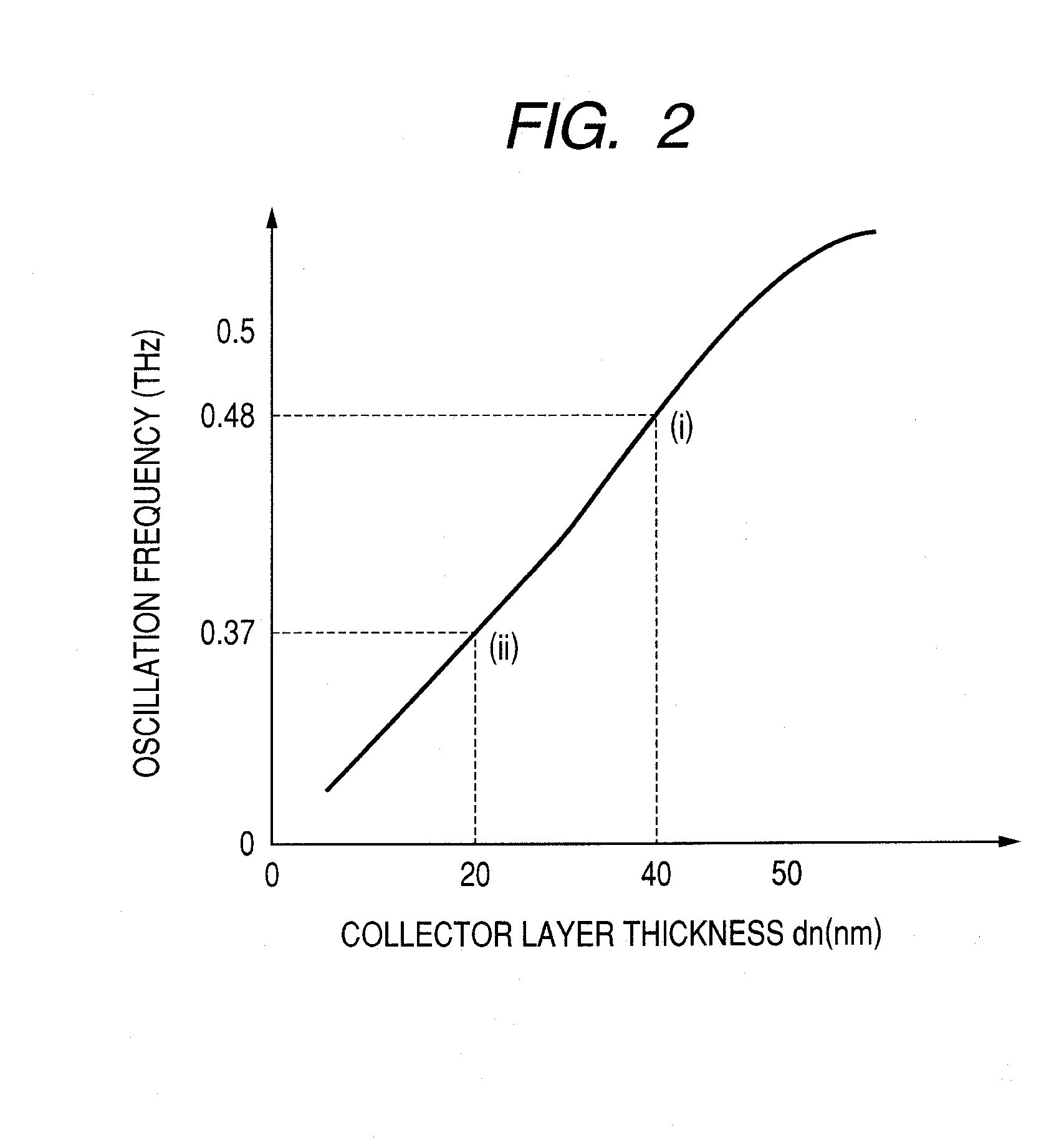
[0076]FIG. 7 is a graph illustrating computation examples for designing the oscillation frequencies of the oscillation device of this example. It illustrates the oscillation frequencies corresponding to the thickness of the thickness adjusting layer that operates as collector when the antenna length is reduced to 30 μm, 15 μm and 10 μm. Note that the semiconductor layer 5 is a post with a width of 1.8 μm and the peak current density is 400 kA / cm2.

[0077]Then, if the antenna length is 30 μm and the thicknesses of the thickness adjusting layers are 40 nm and 20 nm, it will be seen that two oscillation frequencies of 610 GHz and 770 GHz are available. Similarly, a desired two-frequency oscillation device can be provided by selecting desired oscillation frequencies from FIG. 7.

[0078]An oscillation device accordi...


PUM


Abstract

An oscillation device has a resonant tunneling diode formed by interposing a gain medium including a first barrier layer, a quantum well layer and a second barrier layer between a first thickness adjusting layer and a second thickness adjusting layer. The oscillation device also has a switch for switching the polarity of a bias voltage being applied to the resonant tunneling diode. The first thickness adjusting layer and the second thickness adjusting layer have different thicknesses. Thus, a single oscillation device is driven to oscillate with different oscillation frequencies.

Description

BACKGROUND OF THE INVENTION[0001]1. Field of the Invention[0002]This invention relates to a current injection type oscillation device using a frequency region from the millimeter wave to the terahertz wave (from 30 GHz to 30 THz). More particularly, the present invention relates to a current injection type oscillation device having a resonant tunneling diode structure.[0003]2. Description of the Related Art[0004]Non-destructive sensing techniques using electromagnetic waves in a frequency region from the millimeter wave to the terahertz wave (from 30 GHz to 30 THz) (to be referred to simply as “terahertz wave” hereinafter) have been and are being developed. In the field of application of electromagnetic waves of this frequency band, safe imaging techniques have been and are being developed for see-through inspection apparatus that can replace X-ray inspection apparatus. Furthermore, spectroscopic technologies for looking into the physical properties including the bonded status of a ...

Claims


Application Information

Patent Timeline
Patent Type & Authority Applications(United States)
IPC IPC(8): H03B7/08
CPCH03B7/08
Inventor ASADA, MASAHIROOUCHI, TOSHIHIKOSEKIGUCHI, RYOTA
Owner CANON KK
Why Eureka
Try Eureka