
Monolithic silicon wafer gaseous phase HMDS coating device

A coating device and silicon wafer technology, applied in the field of HMDS coating technology, can solve problems such as uneven coating, high processing precision requirements, and high HMDS consumption, and achieve low HMDS flow rate and good coating uniformity Effect

Active Publication Date: 2018-05-29
宁波润华全芯微电子设备有限公司
View PDF4 Cites 6 Cited by
  • Summary
  • Abstract
  • Description
  • Claims
  • Application Information

AI Technical Summary

Problems solved by technology

Solve the problems of high equipment structure and processing precision, high HMDS flow rate and large consumption, and uneven coating during vacuum coating in the past

Method used


Image

  • Monolithic silicon wafer gaseous phase HMDS coating device
  • Monolithic silicon wafer gaseous phase HMDS coating device
  • Monolithic silicon wafer gaseous phase HMDS coating device

Examples


Embodiment 1

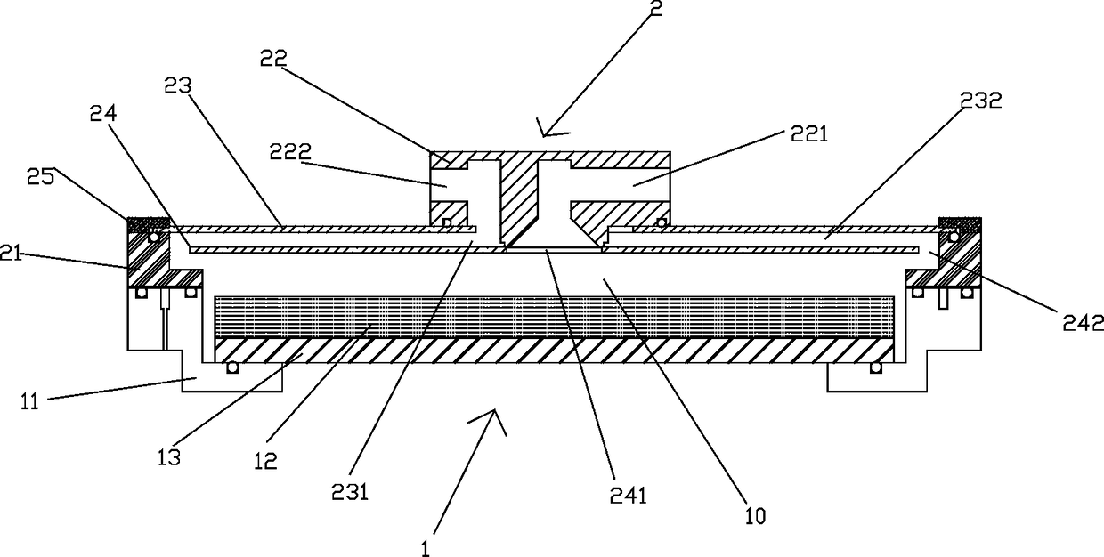
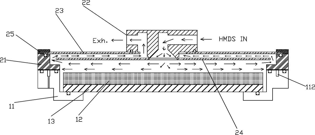
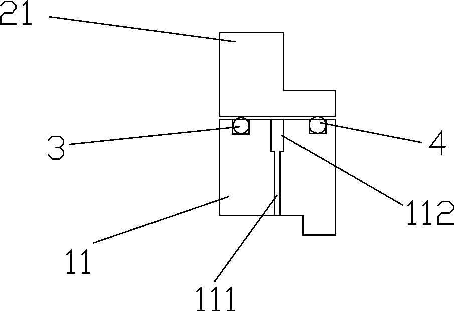
[0023] Example 1, such as Figure 1 to Figure 4 As shown, a vapor-phase HMDS coating device for a single silicon wafer includes a tray assembly 1 and an upper cover assembly 2, the tray assembly 1 and the upper cover assembly 2 are mutually opened and closed, and the tray assembly 1 When it is closed with the upper cover assembly 2, a coating cavity 10 is formed between the two, and the two are sealed. The upper cover assembly 2 includes an upper disc cover 21, the disc body assembly 1 includes a bottom support shield 11, and a gas-tight structure is adopted between the upper cover assembly 2 and the disc body assembly 1, and the gas The sealing structure includes an inner seal 4 and an outer seal 3 arranged between the bottom support shield 11 and the upper plate cover 21, the inner seal 4 and the outer seal 3, there is a gap between them, and the bottom support shield 11 is provided with an annular sealing air channel 112, the annular sealing air channel 112 connects the ga...


PUM


Abstract

The invention relates to a monolithic silicon wafer gaseous phase HMDS coating device, and relates to a semiconductor fabrication technique. The monolithic silicon wafer gaseous phase HMDS coating device comprises a disc assembly and an upper cover assembly, the disc assembly and the upper cover assembly are opened and closed mutually, when the disc assembly and the upper cover assembly are closed, a coating cavity is formed between the disc assembly and the upper cover assembly, and the disc assembly and the upper cover assembly are sealed. The position between the upper cover assembly and the disc assembly adopts a gaseous sealing structure, the gas pressure in the gaseous sealing structure is higher than the pressure in the coating cavity, and an HMDS air inlet channel and an HMDS air outlet channel being communicated with the coating cavity are formed in the upper cover assembly. Coating can be conducted on wafer under an ordinary pressure situation, the flow rate of HMDS is low inthe coating process, the HMDS coating consumption needed by each wafer is only 1.125L to 1.67L, and meanwhile the coating evenness is good. The problems that the requirements for equipment structuresand machining precision in traditional vacuum coating process are high, the flow rate of HMDS is high, consumption of HMDS is large, and coating is not even are solved.

Description

technical field [0001] The invention relates to a semiconductor manufacturing technology, especially a HMDS coating technology. Background technique [0002] In the semiconductor production process, photolithography is the most important link. The uniformity of the gluing process before lithography will directly affect the quality of lithography. In the coating process, most photoresists are hydrophobic, while the hydroxyl groups and residual water molecules on the surface of the silicon wafer are hydrophilic. Therefore, it is necessary to apply a tackifier before coating the glue. The function of the tackifier is to change the hydrophilicity of the silicon wafer to hydrophobicity, thereby increasing the adhesion between the photoresist and the surface of the silicon wafer. HMDS (hexamethyldisilamine) is a commonly used tackifier. HMDS is a colorless transparent liquid at room temperature with an amine-like odor. HMDS is reproductively toxic and highly volatile, so prote...

Claims


Application Information

Patent Timeline
Patent Type & Authority Applications(China)
IPC IPC(8): B05C9/14B05D3/04
CPCB05C9/14B05D3/0486
Inventor 傅立超施科科
Owner 宁波润华全芯微电子设备有限公司
Learn More