GaN-based vertical structure LED device

A technology of LED device and vertical structure, applied in semiconductor devices, electrical components, circuits, etc., can solve the problems of separation of metal substrate and GaN film, low production qualification rate, poor bonding force between GaN and single metal, etc.

Inactive Publication Date: 2018-06-01
BAODING GOLDEN SUNLIGHT POWER EQUIP TECH
View PDF0 Cites 0 Cited by
  • Summary
  • Abstract
  • Description
  • Claims
  • Application Information

AI Technical Summary

Problems solved by technology

[0005] However, the electroplating method still has many bottlenecks to overcome, the most important of which is: after the laser lift-off, the free GaN film will release itself due to the remaining thermal stress in the growth process to produce a degree of warpage, while electroplating Due to the nature of the metal itself, the metal will also produce a degree of warpage. When the two do not match, it is easy to cause the separation of the electroplated metal substrate and the GaN film, which will lead to the failure of the device. Therefore, a single metal substrate The production qualification rate of GaN-based vertical structure LED devices is extremely low, and even if the production is successful, due to the large difference between the warpage of the electroplated single metal substrate and the GaN film warpage, the combination of GaN and single metal in GaN-based vertical structure LED devices The force is poor, it is easy to warp, even separate, and the service life is very short

Method used


Image

  • GaN-based vertical structure LED device
  • GaN-based vertical structure LED device
  • GaN-based vertical structure LED device

Examples


Embodiment 2

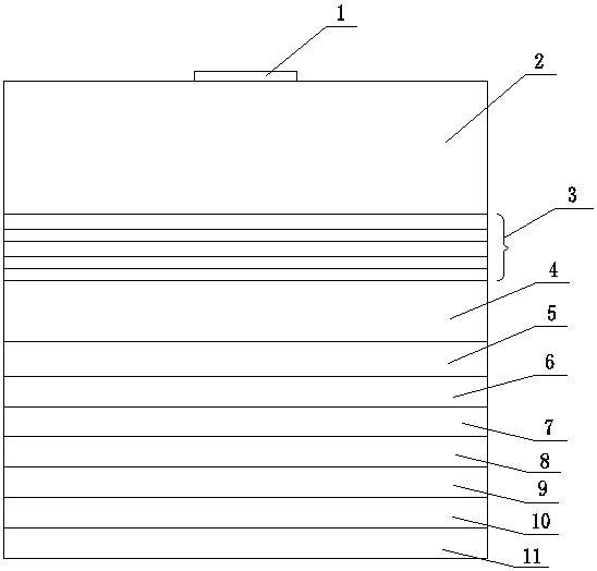
[0016] Such as figure 2 In the shown embodiment 2, this embodiment includes an N electrode 1, an N-type GaN layer 2, a GaN multi-quantum well active layer 3, a P-type GaN layer 4, a P electrode 5 and a metal substrate from top to bottom. Described metal substrate is by the cobalt layer 12 of 25 microns, the tungsten layer 13 of 15 microns, the cobalt layer 14 of 30 microns, the tungsten layer 15 of 40 microns, the cobalt layers 16 and 25 of 25 microns successively from the P electrode to the outside micron tungsten layer 30. The metal substrate has a strong bonding force with the P electrode, and obviously no longer warps.

Embodiment 3

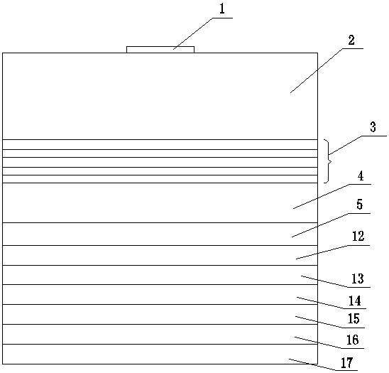
[0017] Such as image 3 In the illustrated embodiment 3, this embodiment includes an N electrode 1, an N-type GaN layer 2, a GaN multi-quantum well active layer 3, a P-type GaN layer 4, a P electrode 5 and a metal substrate from top to bottom. The metal substrate is sequentially composed of a palladium layer of 20 microns, a nickel layer of 18 microns, a palladium layer of 25 microns, a nickel layer of 30 microns, a palladium layer of 40 microns and a nickel layer of 38 microns from the P-GaN electrode to the outside. Layer 30 composition. The metal substrate has a strong bonding force with the P electrode, and obviously no longer warps.

Embodiment 4

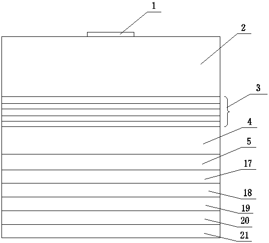
[0018] Embodiment 4, this embodiment includes an N electrode 1, an N-type GaN layer 2, a GaN multi-quantum well active layer 3, a P-type GaN layer 4, a P electrode 5 and a metal substrate from top to bottom. The metal substrate is sequentially composed of a 23-micron gold layer, a 20-micron tungsten layer, a 35-micron gold layer, a 32-micron tungsten layer, a 38-micron gold layer and a 32-micron tungsten layer from the P-GaN electrode to the outside. Layer 30 composition. The metal substrate has a strong bonding force with the P electrode, and obviously no longer warps.


PUM

PropertyMeasurementUnit
thicknessaaaaaaaaaa
thicknessaaaaaaaaaa
thicknessaaaaaaaaaa

Abstract

The invention discloses a GaN-based vertical structure LED device. The device comprises an N electrode, an N type GaN layer, a GaN multi-quantum well active layer, a P type GaN layer, a P electrode and a metal substrate which are distributed sequentially from top to bottom; the metal substrate is of a multi-layer structure; and tensile stress metal layers and compressive stress metal layers are formed alternately through electroplating and fixed so as to form the multi-layer structure. According to the GaN-based vertical structure LED device of the invention, various metal alloys are adopted,so that the adjustment of the support degree of the vertical structure LED device and the substrate can be better facilitated; the strength of connection between plated metal and a GaN film is improved; and the aging characteristic of the vertical structure LED device is improved.

Description

technical field [0001] The invention relates to a vertical structure LED device, in particular to a GaN-based vertical structure LED electroplating metal substrate. Background technique [0002] The Ⅲ / Ⅴ nitride mainly composed of GaN, InGaN, and AlGaN is a semiconductor material that has attracted much attention in recent years. It has a continuously variable direct bandgap of 1.9-6.2eV, excellent physical and chemical stability, and high saturation electron migration. High efficiency and other characteristics make it the most preferred material for optoelectronic devices such as lasers and light-emitting diodes. [0003] However, due to the limitations of GaN's own growth technology, most of today's large-area GaN materials are grown on sapphire substrates. Although the GaN grown on the sapphire substrate is of high quality and the most widely used, due to the non-conductivity of sapphire, the LED device on the sapphire substrate can only be made into a lateral structure i...

Claims


Application Information

Patent Timeline
Patent Type & Authority Applications(China)
IPC IPC(8): H01L33/06H01L33/32H01L33/48
CPCH01L33/06H01L33/32H01L33/48
Inventor 孙永健王光普郭坚张戊有胡勇
Owner BAODING GOLDEN SUNLIGHT POWER EQUIP TECH
Why Eureka
Try Eureka