Manufacturing method of bonding pad structure and manufacturing method of flip LED chip

An LED chip and manufacturing method technology, applied in electrical components, circuits, semiconductor devices, etc., can solve problems such as tin diffusion, and achieve the effects of low cost, simple process, and convenience for mass production

Pending Publication Date: 2018-06-01
HANGZHOU SILAN AZURE
View PDF4 Cites 0 Cited by
  • Summary
  • Abstract
  • Description
  • Claims
  • Application Information

AI Technical Summary

Problems solved by technology

[0005] In view of the above problems, the object of the present invention is to provide a method of manufacturing a pad structure and a method of manufacturing a flip-chip LED chip to solve the problem of tin diffusion during reflow soldering

Method used


Image

  • Manufacturing method of bonding pad structure and manufacturing method of flip LED chip
  • Manufacturing method of bonding pad structure and manufacturing method of flip LED chip
  • Manufacturing method of bonding pad structure and manufacturing method of flip LED chip

Examples


Embodiment 1

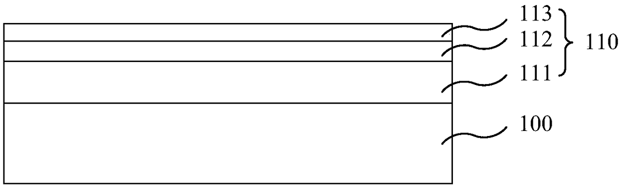
[0059] Such as Figure 1-18 As shown, the flip-chip LED chip includes: a substrate 100, an epitaxial layer 110, a current spreading layer 120, a first connecting electrode 131 and a second connecting electrode 132, an insulating reflective layer 140, a first bonding pad 151 and a second bonding pad. Disk 152.

[0060] The epitaxial layer 110 includes a first semiconductor layer 111, a light emitting layer 112, and a second semiconductor layer 113 formed in sequence, and at least one groove 110a is disposed on the epitaxial layer 110, and the depth of the groove 110a is greater than that of the light emitting layer. layer 112 and the thickness of the second semiconductor layer 113 is less than the thickness of the epitaxial layer 110, that is, the light emitting layer 112 and the second semiconductor layer 113 in the groove 110a are completely removed, while the first semiconductor layer 111 A part is removed, and the present invention does not limit the shape of the groove 11...


PUM


Abstract

The present invention discloses a manufacturing method of a bonding pad structure. The bonding pad structure is applied to a flip LED chip, and the flip LED chip comprises a substrate, an epitaxial layer, a current extension layer, a communication electrode, an insulation reflection layer and a bonding pad structure which are arranged from top to bottom. The manufacturing method of the bonding padstructure comprises the steps of: forming a first contact layer on the insulation reflection layer through an evaporation or sputtering mode; forming a barrier layer on the first contact layer through an electroplating or chemical plating mode; and forming an eutectic layer through an electroplating, chemical plating or thermal resistance evaporation mode, wherein, the thickness of the barrier layer is 0.5-5 [Mu]m, the roughness is 10-30nm. The present invention further provides a manufacturing method of a flip LED chip. The problem is solved that tin is expanded to the surface of the chip ina reflow soldering process, and therefore, the manufacturing method of the bonding pad structure and the manufacturing method of the flip LED chip are simple in technology, low in cost and are convenient for batch production.

Description

technical field [0001] The invention relates to the technical field of semiconductor optoelectronic chip manufacturing, in particular to a method for manufacturing a pad structure and a method for manufacturing a flip-chip LED chip. Background technique [0002] Since its commercialization in the early 1990s, after more than 20 years of development, GaN-based LEDs have been widely used in indoor and outdoor display screens, lighting sources for projection displays, backlight sources, landscape lighting, advertising, traffic instructions, etc. Field, and known as the most competitive new generation of solid-state light source in the 21st century. However, for LEDs to replace traditional light sources and enter the field of high-end lighting, the improvement of their luminous brightness is crucial. [0003] The basic structure of the flip-chip LED chip is to flip-chip-weld the front-mounted LED chip on a substrate with good electrical and thermal conductivity, so that the lig...

Claims


Application Information

Patent Timeline
Patent Type & Authority Applications(China)
IPC IPC(8): H01L33/62H01L33/60H01L33/00H01L33/14H01L33/40
CPCH01L33/005H01L33/14H01L33/40H01L33/60H01L33/62H01L2933/0058H01L2933/0066
Inventor 李东昇丁海生马新刚赵进超
Owner HANGZHOU SILAN AZURE
Why Eureka
Try Eureka