

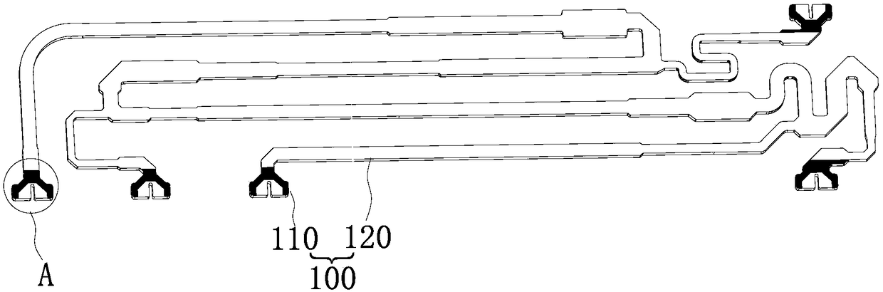
Welding point structure and welding structure of metal conductor microwave network circuit
A microwave network and metal conductor technology, applied in printed circuits, printed circuits, printed circuit manufacturing, etc., can solve the problem of poor stability and shape consistency of tin stacking, excessive solder flow at circuit solder joints, and incomplete coating of cable core wires. and other problems, to achieve the effect of good electrical connection quality, reduction of secondary workload, and improvement of assembly efficiency
- Summary
- Abstract
- Description
- Claims
- Application Information
AI Technical Summary
Problems solved by technology
Method used
Image

Examples
Embodiment Construction
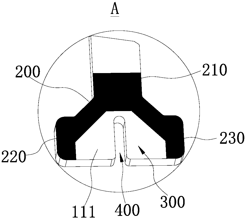
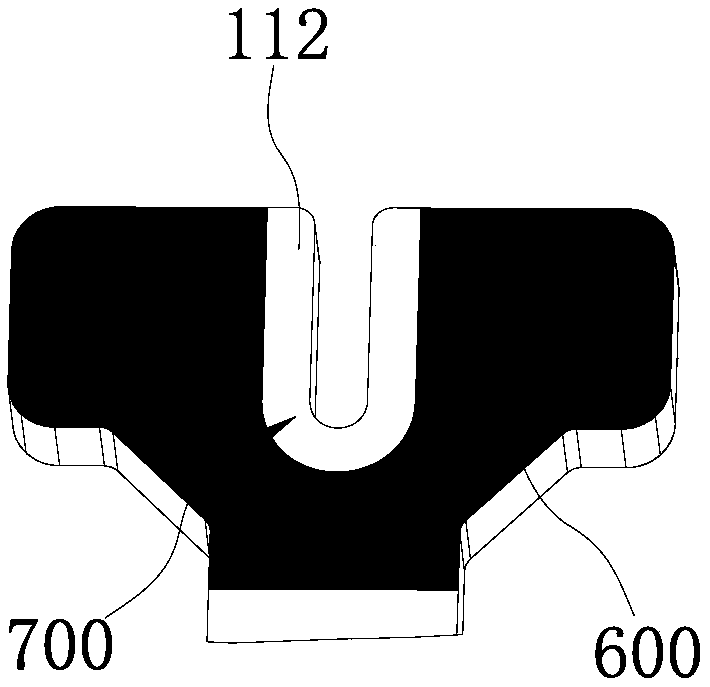
[0028] In order to make the object, technical solution and advantages of the present invention clearer, the present invention will be further described in detail below in conjunction with the accompanying drawings and specific implementation methods. It should be understood that the specific embodiments described here are only used to explain the present invention, and do not limit the protection scope of the present invention.
[0029] It should be noted that when an element is referred to as being “fixed on”, “disposed on” or “installed on” another element, it may be directly on the other element or may also exist as an element therein. When an element is considered to be "connected" to another element, it may be directly connected to the other element or there may be elements in it at the same time; the specific way that an element is fixedly connected to another element can be realized through existing technologies, and will not be discussed here. To repeat it again, it is...
PUM
| Property | Measurement | Unit |
|---|---|---|
| Width | aaaaa | aaaaa |
Abstract
Description
Claims
Application Information