NandFlash address mapping and block management algorithm

A technology of address mapping and block management, which is applied in computing, electrical digital data processing, and input/output process of data processing, etc. It can solve problems such as slowing down disk read and write speed, hidden dangers of data reliability, and limited erasure times

Active Publication Date: 2018-06-05
HONGQIN (BEIJING) TECHNOLOGY CO LTD
View PDF9 Cites 16 Cited by
  • Summary
  • Abstract
  • Description
  • Claims
  • Application Information

AI Technical Summary

Problems solved by technology

[0015] The present invention provides a kind of NandFlash address mapping and block management method, has solved the problem of using NandFlash efficiently, because the characteristic of NandFlash chip, as storage organization structure with page, block (currently NandFlash chip generally every page is 2K or 4K byte , each block has 64 pages), the erasing operation must be performed before rewriting the data, the erasing is in the unit of "block", and the number of erasing is limited, bad blocks will appear during use, etc.; while the operating system accesses the disk It is carried out

Method used


Image

  • NandFlash address mapping and block management algorithm
  • NandFlash address mapping and block management algorithm
  • NandFlash address mapping and block management algorithm

Examples


Embodiment Construction

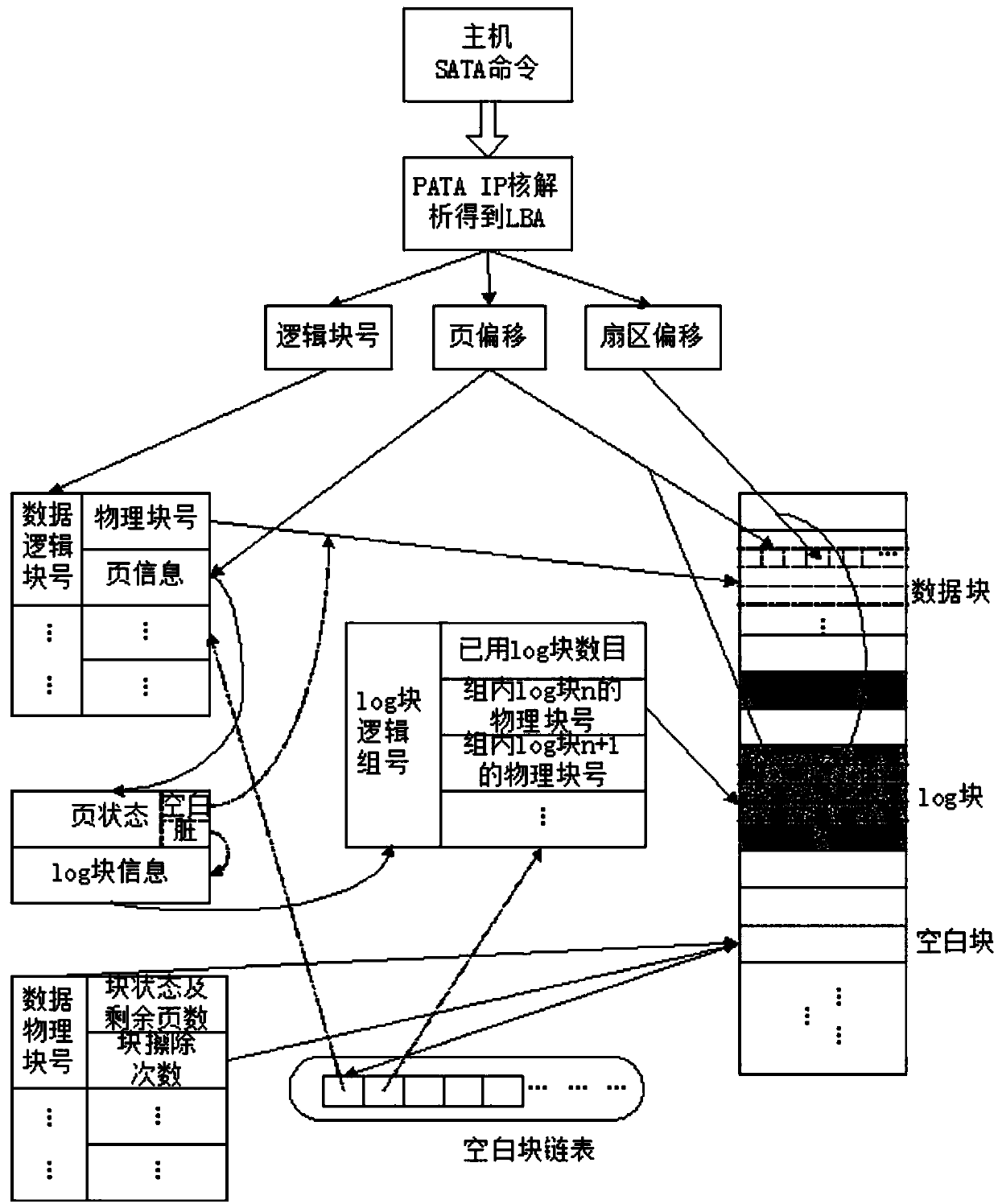
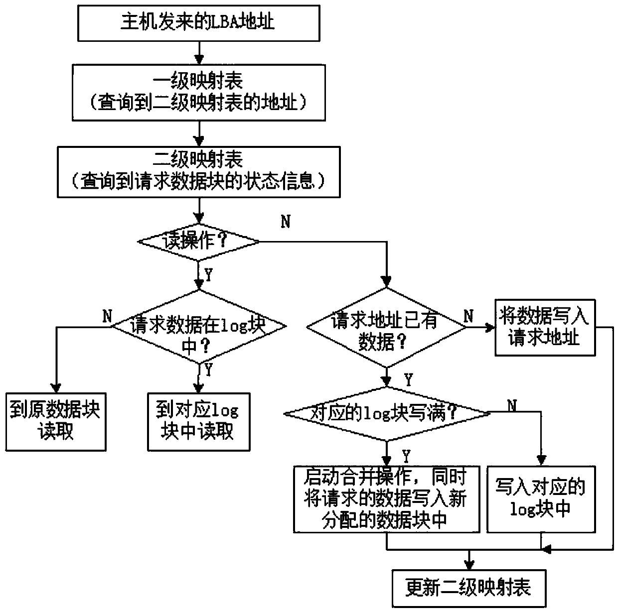
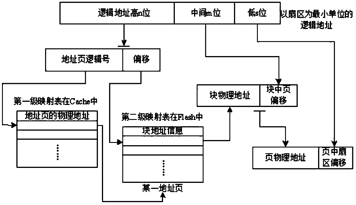
[0049] NandFlash address mapping provided by the invention and block management algorithm comprise the following steps:

[0050] (1) The entire NandFlash chip space is functionally divided into three parts: the storage mapping table information part, the user data storage part and the blank part. The data operation of the three parts is performed using the block management algorithm. The block management algorithm divides the entire NandFlash array according to the physical space and logic space management;

[0051] The physical space is the actual NandFlash storage medium, and each storage block unit of the NandFlash chip is called a physical block, and is numbered sequentially; the physical block without storing data corresponds to a blank part;

[0052] The logical space includes: 1) data logic block, used to store user data, and convert the sector address sent by the host into a corresponding block number according to the block size of the NandFlash chip, called the logica...


PUM


Abstract

The invention provides a NandFlash address mapping and a block management algorithm. The NandFlash address mapping and the block management algorithm are a part of the firmware design of a solid-statedisc controller, and mainly play the following roles: 1, the address information taking a sector as a unit sent by a mainframe is translated into a physical block and a page address of a NandFlash chip; 2, each block of the NandFlash chip is used as evenly as possible through the block management algorithm, the usage rate of each block is improved, the unnecessary erasure operations are avoided,the number of times of the block erased is reduced, which is commonly known as load balancing; 3, the bad blocks are managed in the using process to ensure the reliability of data; 4, optimized NandFlash multi-channel address mapping design is adopted to realize multi-channel parallel/pipeline operations.

Description

technical field [0001] The invention relates to the field of storage technology, in particular to a NandFlash address mapping and block management method. Background technique [0002] NAND Flash can greatly reduce the cost per bit of flash memory by reducing the process size and adopting multi-level technology, but this also brings other problems, mainly manifested in the degradation of device performance: such as decreased access speed, increased bit error rate, durability degree of degradation and deterioration of retention characteristics, etc. Among them, endurance refers to the maximum programming and erasing times (P / E Cycles) that a memory cell can withstand. The reason why there is a maximum number of times of erasing and writing is that the programming and erasing operations of flash memory are carried out through the electron tunneling mechanism, and a large number of tunneling will cause stress on the tunneling oxide layer, resulting in the electrical performanc...

Claims


Application Information

Patent Timeline
IPC IPC(8): G06F3/06
CPCG06F3/0614G06F3/064G06F3/0644G06F3/0656G06F3/0679G06F2212/7201G06F12/0246
Inventor 蔡震杨建利张涛周洋
Owner HONGQIN (BEIJING) TECHNOLOGY CO LTD
Why Eureka
Try Eureka