Thin film transistor and manufacturing method thereof, array substrate and display device

A technology of a thin film transistor and a manufacturing method, applied in the field of array substrates and display devices, thin film transistors and manufacturing methods thereof, capable of solving the problems of high parasitic resistance at the source and drain terminals and large ohmic contact resistance of top-gate thin film transistors, and reducing the Small parasitic resistance and total source-drain resistance, saving time and energy consumption, and improving device performance

Active Publication Date: 2018-06-05
BOE TECH GRP CO LTD
View PDF3 Cites 4 Cited by
  • Summary
  • Abstract
  • Description
  • Claims
  • Application Information

AI Technical Summary

Problems solved by technology

[0004] The present invention provides a thin film transistor and its manufacturing method, an array substrate and a display device, which are used to solve the problem of large parasitic resistance of the source and drain terminals of the top gate type thin film transistor caused by the existing manufacturing process, and the problem of the connection between the source electrode and the drain electrode and the active layer. The problem of large ohmic contact resistance

Method used


Image

  • Thin film transistor and manufacturing method thereof, array substrate and display device
  • Thin film transistor and manufacturing method thereof, array substrate and display device
  • Thin film transistor and manufacturing method thereof, array substrate and display device

Examples


Embodiment 1

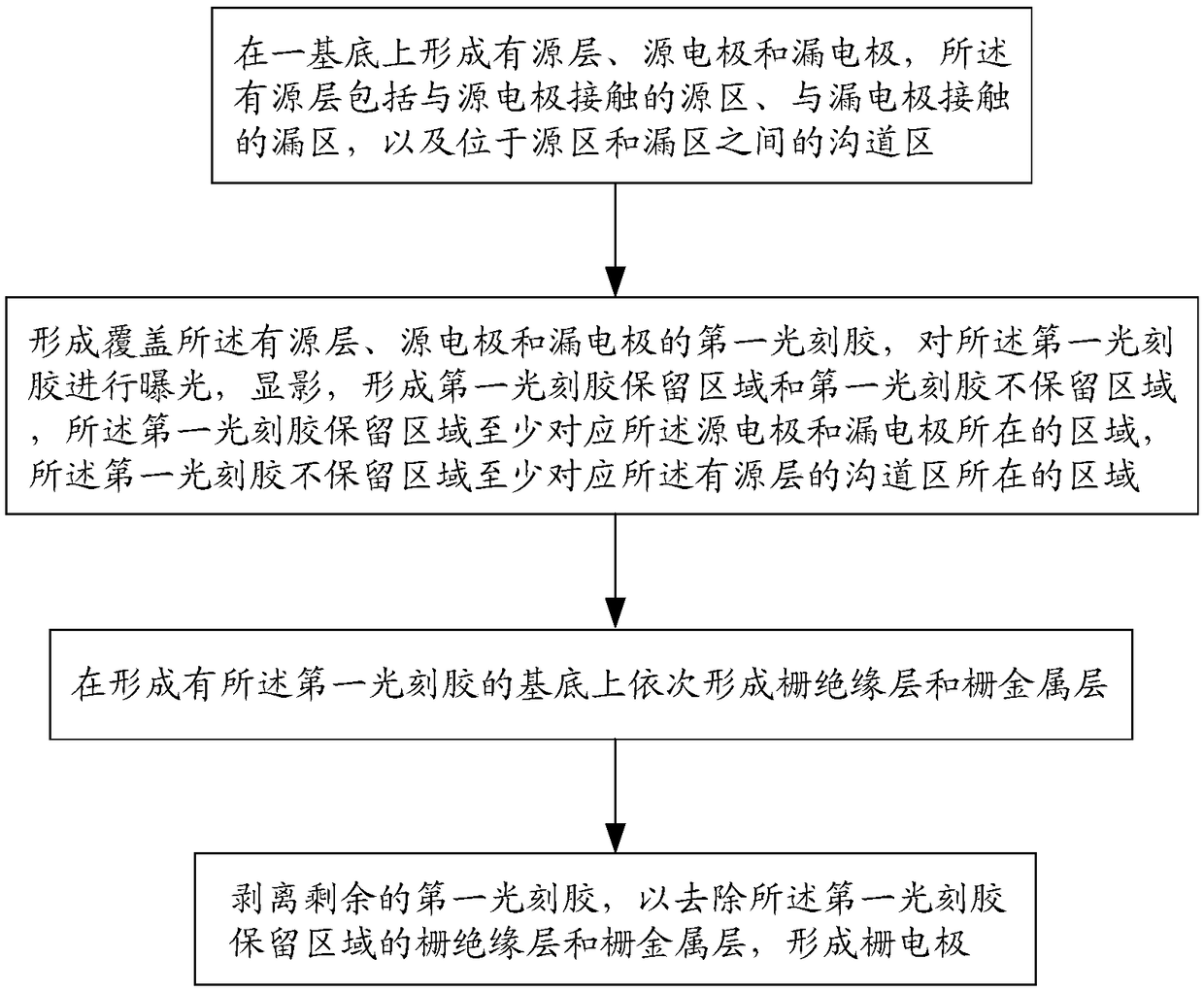
[0023] like figure 1 As shown, a method for manufacturing a thin film transistor is provided in this embodiment, specifically a method for manufacturing a top-gate thin film transistor, and the method includes:

[0024] Forming an active layer, a source electrode and a drain electrode on a substrate, the active layer including a source region in contact with the source electrode, a drain region in contact with the drain electrode, and a channel region between the source region and the drain region ;

[0025] Forming a first photoresist covering the active layer, source electrode and drain electrode, exposing and developing the first photoresist to form a first photoresist remaining area and a first photoresist non-retaining area , the first photoresist-retained region at least corresponds to the region where the source electrode and the drain electrode are located, and the first photoresist-free region corresponds to at least the region where the channel region of the active ...

Embodiment 2

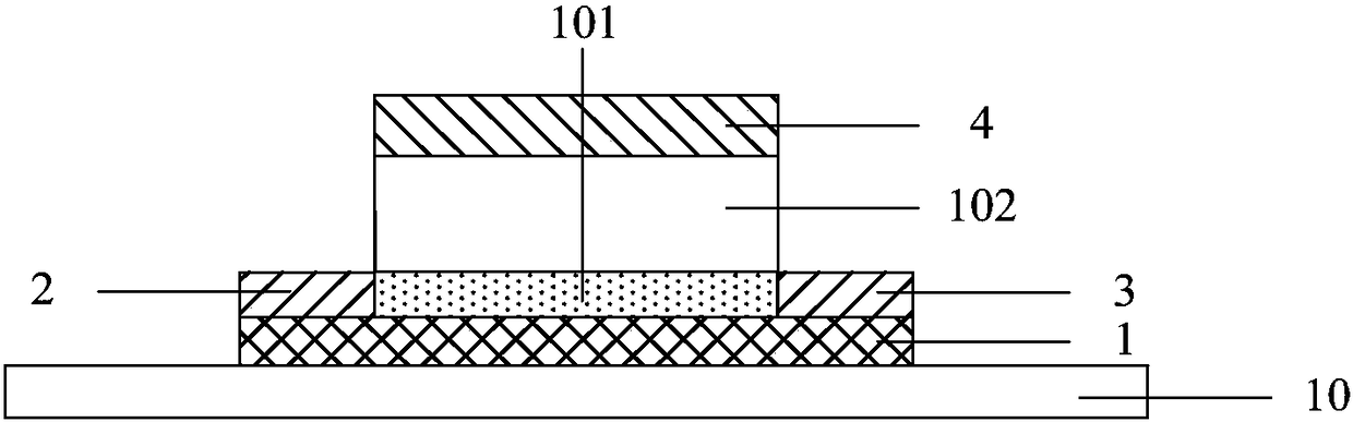
[0065] like figure 2 As shown, this embodiment provides a thin film transistor manufactured by the manufacturing method in Embodiment 1, including:

[0066] An active layer 1, a source electrode 2 and a drain electrode 3 arranged on a substrate 10, the active layer 1 includes a source region in contact with the source electrode 2, a drain region in contact with the drain electrode 3, and a region located in the source region and the drain region channel region between

[0067] A gate insulating layer disposed on the active layer 1 and a gate electrode 4 disposed on the gate insulating layer, wherein the patterns of the gate insulating layer and the gate electrode 4 are consistent, and the gate insulating layer includes The first part between the electrode and the drain electrode, the orthographic projection of the first part on the substrate coincides with the orthographic projection of the channel region of the active layer on the substrate.

[0068] The source electrode, ...

Embodiment 3

[0078] This embodiment provides an array substrate and a display device, the array substrate adopts the thin film transistor in Embodiment 2, and the display device includes the thin film transistor. The thin film transistor is specifically a top-gate thin film transistor. Since the gate electrode is self-aligned with the source electrode and the drain electrode, the alignment is strict and accurate, which reduces the parasitic resistance of the device and the total resistance of the source and drain, improves the performance of the device, and improves In order to display the display quality of the product. At the same time, it saves the process steps of separately making the gate, saves the process, and also saves the process of conducting the active layer, saves time and energy consumption, and overcomes the limitations of the material selection of the source electrode and the drain electrode. The problem of limiting the ohmic contact resistance of the source layer reduces ...


PUM


Abstract

The invention relates to the technical field of display, and discloses a thin film transistor and a manufacturing method thereof, an array substrate and a display device. The manufacturing method comprises steps: firstly, an active layer, a source electrode and a drain electrode of the thin film transistor are formed; the graph of a first photoresist is then formed, wherein the first photoresist covers the area of the source electrode and the drain electrode, is in position correspondence with the source electrode and the drain electrode and has the consistent graph; and finally, a gate insulation layer and a gate metal layer are sequentially formed on the first photoresist, through a process of stripping the first photoresist, the gate insulation layer and the gate metal layer above the first photoresist are removed, a gate electrode is formed, self alignment between the gate electrode and the source electrode and the drain electrode is realized, contraposition is strict and accurate,parasitic resistance of the device and the total source-drain resistance are reduced, the device performance is improved, and the display quality of a display product is enhanced, and besides, the procedure is saved, time and energy consumption are saved, and the production cost is reduced.

Description

technical field [0001] The invention relates to the field of display technology, in particular to a thin film transistor and a manufacturing method thereof, an array substrate and a display device. Background technique [0002] In the field of flat panel display technology, thin film transistors (Thin Film Transistor, TFT for short) have the advantages of small size, low power consumption, and relatively low manufacturing cost, and are widely used as driving devices in flat panel display technology. [0003] Because there is no overlapping area between the gate electrode and the source electrode and the drain electrode, the top-gate thin film transistor has relatively small parasitic capacitance, which is reflected in the pixel circuit and has a higher switching speed, so it is doubled in large-size display products. favored. However, the main problems currently existing in the top gate thin film transistor include: 1) The gate electrode is prepared by a wet etching process...

Claims


Application Information

Patent Timeline
Patent Type & Authority Applications(China)
IPC IPC(8): H01L21/336H01L21/34H01L21/28H01L29/423H01L29/786
CPCH01L29/401H01L29/42384H01L29/66757H01L29/66969H01L29/78603H01L29/78675H01L29/7869H01L29/41733H01L29/45H01L29/458H01L29/4908H01L21/0273H01L29/42316H01L29/66742H01L29/78618H01L29/78696H01L29/423H01L29/1033
Inventor 宋振李伟王国英
Owner BOE TECH GRP CO LTD
Why Eureka
Try Eureka