NMOS transistor structure and forming method thereof

A transistor and gate structure technology, applied in the manufacture of transistors, semiconductor devices, semiconductor/solid-state devices, etc., can solve the problems of deteriorating the threshold voltage of transistor devices, shortening the channel length, and the device cannot be turned off, and achieves a process result that can be Strong controllability, improved on-current, and optimized device performance

Active Publication Date: 2018-06-08
江苏芯长征微电子集团股份有限公司 +1
View PDF4 Cites 3 Cited by
  • Summary
  • Abstract
  • Description
  • Claims
  • Application Information

AI Technical Summary

Problems solved by technology

[0002] In the existing semiconductor structure, with the continuous reduction of the feature size of MOS devices, the length of the channel becomes shorter, and the width will also be reduced in the same proportion, which will lead to serious short channel effect.
This is because when a high voltage is applied to the drain, since the gate is very short, the source is also affected by the electric field of the drain. The depletion region of the junction is connected, so the device cannot be turned off, resulting in a large leakage current
As the channel length is further shortened, the short channel effect is more obvious, which seriously deteriorates the threshold voltage of transistor devices

Method used


Image

  • NMOS transistor structure and forming method thereof
  • NMOS transistor structure and forming method thereof
  • NMOS transistor structure and forming method thereof

Examples


Embodiment Construction

[0018] In order to make the purpose, technical solutions and advantages of the present invention more clearly understood, the specific embodiments of the present invention will be further described in detail below in conjunction with the accompanying drawings.

[0019] The present invention may be embodied in many different forms and should not be construed as limited to the embodiments described herein. It will be understood that when an element such as a layer, region, or substrate is referred to as being "formed on" or "disposed on" another element, it can be directly on the other element or be directly on the other element. There are intermediate elements.

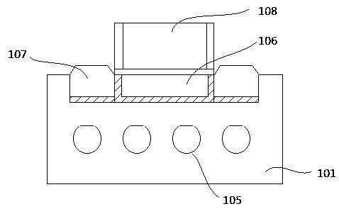
[0020] Such as figure 1 As shown, the NMOS transistor structure of the present invention includes: a substrate 101, a spherical blocking device 105 located in the substrate, the spherical blocking device can effectively weaken the coupling capacitance between the source and the drain, and reduce the The current leaka...


PUM


Abstract

The invention discloses an NMOS transistor structure and a forming method thereof, which relate to the technical field of basic electronic components. The transistor comprises a substrate, a gate structure, a channel region and a source and drain region. The semiconductor structure further comprises a spherical blocking device, and a carbon-containing material layer located at the interface of thesubstrate and the channel region and at the interface of the substrate and the source and drain region. The spherical blocking device is arranged in the substrate and located below the source and drain region and the channel region. The spherical blocking device is an empty cavity or is filled with an insulating medium. The weight ratio of carbon atoms to silicon atoms in the carbon-containing material layer below the channel region is 1: (0.7-2.4). The leakage current of the semiconductor structure is significantly reduced, and the electrical performance is obviously improved. The method offorming the semiconductor structure has the advantages of simple process, low cost and less impurity introduced, and can further improve the performance of the semiconductor structure.

Description

technical field [0001] The present application relates to the field of semiconductors, in particular to semiconductor structures and methods for forming them, NMOS transistors and methods for forming them. Background technique [0002] In the existing semiconductor structure, as the feature size of MOS devices decreases continuously, the length of the channel becomes shorter, and the width will also be reduced in the same proportion, which will lead to serious short channel effect. This is because when a high voltage is applied to the drain, since the gate is very short, the source is also affected by the electric field of the drain. The depletion region of the junction is connected, so the device cannot be turned off, resulting in a large leakage current. As the channel length is further shortened, the short-channel effect becomes more obvious, which seriously deteriorates the threshold voltage of transistor devices. [0003] In order to solve the above-mentioned technica...

Claims


Application Information

Patent Timeline
Patent Type & Authority Applications(China)
IPC IPC(8): H01L29/06H01L29/16H01L29/78H01L21/336
CPCH01L29/0638H01L29/0649H01L29/0684H01L29/16H01L29/66568H01L29/78
Inventor 孟静
Owner 江苏芯长征微电子集团股份有限公司
Why Eureka
Try Eureka