Constant current device and manufacturing method thereof
A technology of constant current device and manufacturing method, applied in semiconductor devices, electrical components, transistors, etc., to achieve the effect of large current density, increase flexibility, and avoid the problem of reverse voltage resistance
- Summary
- Abstract
- Description
- Claims
- Application Information
AI Technical Summary
Problems solved by technology
Method used
Image
Examples
Embodiment 1
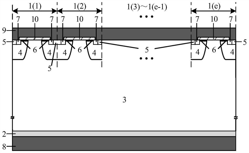
[0061] A constant current device, including two parts, a cell area and a terminal area, the cell area includes a plurality of cells 1(1), 1(2)...1(e) with the same structure and sequentially connected, each The cell includes a P-type doped substrate 2, an N-type inverse doped well region 3, and a diffused P-type well region 4 located in the N-type inversely doped well region 3, and the diffused P-type well region 4 is two and are respectively located at both ends of each cell, the diffused P-type well region 4 is provided with a first P-type heavily doped region 5 and an N-type heavily doped region 7, and the N-type heavily doped region 7 is located in the first P-type On both sides of the heavily doped region 5, an oxide layer 10 is provided on the upper surface of the N-type reverse doped well region 3 and the diffused P-type well region 4, and an N-type The depletion channel region 6, the cell region also includes a metal cathode 9 covering the entire upper surface of the c...
Embodiment 2
[0081] Such as Figure 4 As shown, the difference between this embodiment and Embodiment 1 is that the terminal region also includes a P-type doped ring region 41 located at the inner edge of the N-type reverse doped well region 3, and the diffused P-type well region 4 and The P-type doped ring regions 41 are connected into one body.
[0082] The number e of the cells can be adjusted according to specific current capability requirements; the thickness of the substrate can be adjusted according to specific current capability and voltage withstand capability requirements.
[0083] The distance between the diffused P-type well regions 4 in the cells, the thickness of the substrate and the number of cells can be adjusted according to the requirements of specific withstand voltage and pinch-off voltage, which greatly increases the flexibility of device design.
[0084] Said cells form a thin-layer channel by implanting phosphorus ions on the surface of the diffused P-type well reg...
PUM
| Property | Measurement | Unit |
|---|---|---|
| thickness | aaaaa | aaaaa |
| thickness | aaaaa | aaaaa |
Abstract
Description
Claims
Application Information


