Constant current device and manufacturing method thereof
A technology of constant current devices and manufacturing methods, applied to semiconductor devices, electrical components, transistors, etc., to achieve the effects of saving chip area, avoiding the problem of reverse non-voltage resistance, and stabilizing the current value
- Summary
- Abstract
- Description
- Claims
- Application Information
AI Technical Summary
Problems solved by technology
Method used
Image
Examples
Embodiment 1
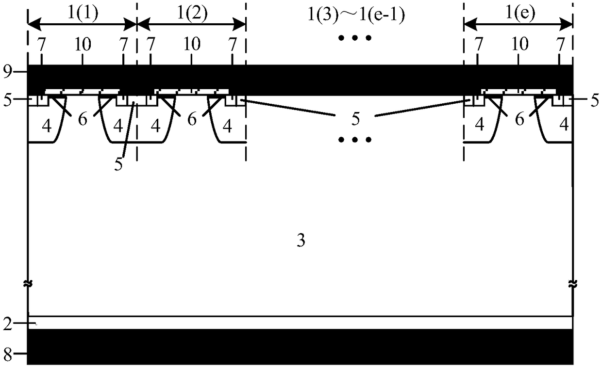
[0061] A constant current device, including two parts, a cell area and a terminal area, the cell area includes a plurality of cells 1(1), 1(2)...1(e) with the same structure and sequentially connected, each The cell includes a P-type doped substrate 2, an N-type inverse doped well region 3, and a diffused P-type well region 4 located in the N-type inversely doped well region 3, and the diffused P-type well region 4 is two and are respectively located at both ends of each cell, the diffused P-type well region 4 is provided with a first P-type heavily doped region 5 and an N-type heavily doped region 7, and the N-type heavily doped region 7 is located in the first P-type On both sides of the heavily doped region 5, an oxide layer 10 is provided on the upper surface of the N-type reverse doped well region 3 and the diffused P-type well region 4, and an N-type The depletion channel region 6, the cell region also includes a metal cathode 9 covering the entire upper surface of the c...
Embodiment 2
[0081] like Figure 4 As shown, the difference between this embodiment and Embodiment 1 is that the terminal region also includes a P-type doped ring region 41 located at the inner edge of the N-type reverse doped well region 3, and the diffused P-type well region 4 and The P-type doped ring regions 41 are connected into one body.
[0082] The number e of the cells can be adjusted according to specific current capability requirements; the thickness of the substrate can be adjusted according to specific current capability and voltage withstand capability requirements.
[0083] The distance between the diffused P-type well regions 4 in the cells, the thickness of the substrate and the number of cells can be adjusted according to the requirements of specific withstand voltage and pinch-off voltage, which greatly increases the flexibility of device design.
[0084] Said cells form a thin-layer channel by implanting phosphorus ions on the surface of the diffused P-type well region...
PUM
 Abstract
Description
Claims
Application Information


