Constant current device and manufacturing method thereof
A constant current device, N-type technology, applied in semiconductor/solid-state device manufacturing, semiconductor devices, electrical components, etc., to achieve the effect of saving chip area, low cost, and avoiding reverse voltage failure
- Summary
- Abstract
- Description
- Claims
- Application Information
AI Technical Summary
Problems solved by technology
Method used
Image
Examples
Embodiment 1
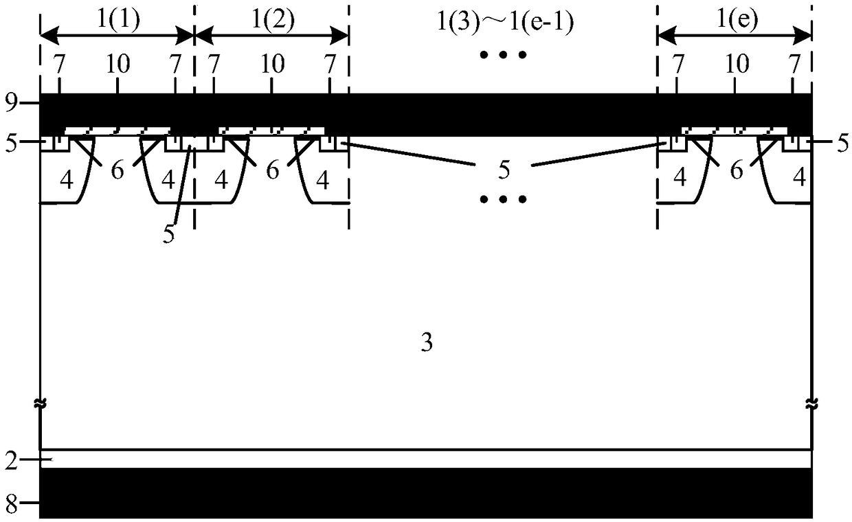
[0080] A constant current device, including a plurality of cells with the same structure and sequentially connected, each cell includes a P-type heavily doped substrate 2, an N-type doped epitaxial layer 3, and is located in the N-type doped epitaxial layer 3 The diffused P-type well region 4, the diffused P-type well region 4 is two and respectively located at both ends of each cell, the first P-type heavily doped region 5 and N located inside the diffused P-type well region 4 Type heavily doped region 7, the first P type heavily doped region 5 is located on both sides of the N type heavily doped region 7, an oxide layer 10 is provided on the upper surface of the N type doped epitaxial layer 3 and the diffused P type well region 4, The cell also includes a metal cathode 9 covering the entire upper surface of the cell, a metal anode 8 located on the lower surface of the P-type heavily doped substrate 2, the first P-type heavily doped region 5, the N-type heavily doped region 7 ...
Embodiment 2
[0099] Such as Figure 4 As shown, the difference between this embodiment and Embodiment 1 is that the constant current device also includes a P-type doped ring region 41 located at the inner edge of the cell region, and a diffused P-type well region 4 and a P-type well region at the outermost edge of the entire device. The doped ring region 41 is connected as a whole.
[0100] In this embodiment, there is no dielectric 13 inside the deep dielectric trench 12 for filling the gap of the oxide layer in the trench.
[0101] Such as Figure 7(1)-Figure 7(10) As shown, FIG. 7 is a schematic flow chart of the manufacturing method of the constant current device provided in this embodiment. Among them, Figure 7(1) is the initial silicon wafer; Figure 7(2) is the silicon wafer after N-type doped epitaxy on the front; Figure 7(3) is the deep groove etched in the epitaxial wafer terminal area; Figure 7(4) In order to perform P-type impurity implantation on the bottom of the groove; Fi...
Embodiment 3
[0103] Such as Figure 9As shown, the difference between this embodiment and Embodiment 3 is that: the dielectric deep groove 12 is provided with a dielectric 13 for filling the gap of the oxide layer in the groove.
[0104] As a preferred manner, each doping type in the constant current device is correspondingly changed to opposite doping, that is, when P-type doping changes to N-type doping, N-type doping changes to P-type doping.
[0105] As a preferred manner, the semiconductor material used in the constant current device is silicon or silicon carbide.
[0106] Further, the P-type doped ring region 41 in the constant current device can be one or more according to the difference of the withstand voltage of the device.
[0107] Further, the bottom of the groove in the constant current device does not necessarily need to be in the P-type heavily doped substrate 2 , it only needs to meet the requirement that the PN junction at the bottom of the groove is connected to the P-ty...
PUM
 Abstract
Description
Claims
Application Information


