A method for manufacturing semiconductor packaging devices by laser

A technology for packaging devices and semiconductors, used in semiconductor/solid-state device manufacturing, manufacturing tools, laser welding equipment, etc., can solve problems such as failure to achieve device design goals, high process complexity, and poor process accuracy, saving space. , The effect of low production complexity and improved efficiency

Active Publication Date: 2019-10-11
丽智电子(南通)有限公司
View PDF5 Cites 0 Cited by
  • Summary
  • Abstract
  • Description
  • Claims
  • Application Information

AI Technical Summary

Problems solved by technology

At present, the manufacturing methods of packaging devices in the electronics industry are mostly traditional mechanical processing. For device processing of high-end semiconductor components such as diodes, there may be poor process accuracy, high process complexity, or even failure to achieve device design purposes.

Method used


Image

  • A method for manufacturing semiconductor packaging devices by laser
  • A method for manufacturing semiconductor packaging devices by laser
  • A method for manufacturing semiconductor packaging devices by laser

Examples


Embodiment Construction

[0029] The present invention will be further described below in conjunction with the accompanying drawings. The following examples are only used to illustrate the technical solution of the present invention more clearly, but not to limit the protection scope of the present invention.

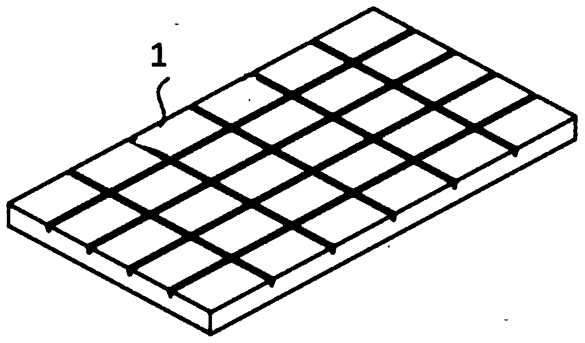
[0030] Such as figure 1 Shown, a kind of laser manufactures the method for semiconductor packaging device, comprises the following steps:

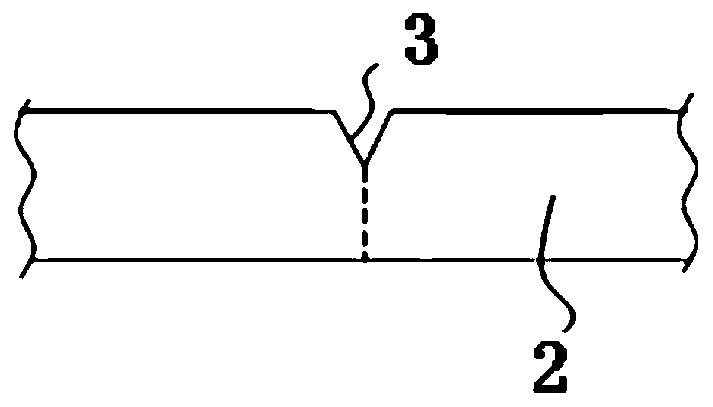
[0031] Step 1, such as figure 1 and 2 As shown, grooves 3 are cut on the top surface of the ceramic substrate 2. The cross section of the grooves 3 is V-shaped. The grooves 3 include several horizontal and several vertical ones. Several component units 1 are formed by dividing the grooves 3. Define The module unit 1A side is opposite to the B side.

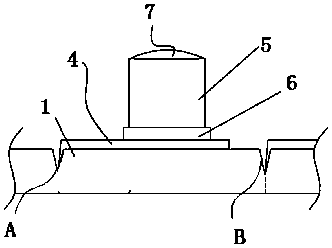
[0032] Step 2, such as image 3 As shown, the top surface of the assembly unit 1 is coated with conductive paste, and extends to the side of the assembly unit 1A to form the lower conductive path 4 .

[00...


PUM


Abstract

The invention discloses a method for manufacturing a semiconductor encapsulation device by laser. In combination with a laser technology, as a semiconductor is encapsulated by a ceramic material serving as a substrate, the precision is high, and the manufacturing complexity is relatively low; meanwhile, an end electrode is provided for the encapsulation device, and can be directly assembled to anelectrical appliance module; and therefore, the space is saved, and the assembling efficiency of the electrical appliance module is improved.

Description

technical field [0001] The invention relates to a method for manufacturing a semiconductor packaging device by laser, belonging to the field of semiconductor packaging. Background technique [0002] With the continuous development of science and technology, the speed of updating and iterating electronic products is also accelerating. Semiconductor component packaging technology is integrated with advanced technologies in other fields, and is developing towards miniaturization and high-efficiency production. At present, the manufacturing methods of packaged devices in the electronics industry are mostly traditional mechanical processing. For the device processing of high-end semiconductor components such as diodes, the process accuracy is poor, the process complexity is high, and even the device design purpose cannot be achieved. Contents of the invention [0003] In order to solve the above technical problems, the present invention provides a method for laser manufacturing...

Claims


Application Information

Patent Timeline
Patent Type & Authority Patents(China)
IPC IPC(8): H01L21/56H01L21/48B23K26/402
CPCB23K26/402H01L21/4857H01L21/56
Inventor 王焕菊褚宏深王国庆宋旭官黄正信
Owner 丽智电子(南通)有限公司
Why Eureka
Try Eureka