3D assembling method for integrally integrating chips of T/R assembly

An assembly method and chip technology, applied in the fields of semiconductor/solid-state device manufacturing, electric solid-state devices, semiconductor devices, etc., can solve the problem of unsuitable T/R component design and assembly, no telecommunication signal chip design combination, no transmitting function and receiving function. function and other issues, to achieve the effect of fast signal transmission, reduced volume and weight, and reduced size

Inactive Publication Date: 2015-02-04
10TH RES INST OF CETC
View PDF3 Cites 47 Cited by
  • Summary
  • Abstract
  • Description
  • Claims
  • Application Information

AI Technical Summary

Problems solved by technology

It is divided into two forms: one is the stacking of CSP / BGA packaged chips and chips, and the other is to use the bottom space of QFP packaged large chips to assemble 0201 micro-packaged resistive capacitor devices to realize the assembly of chips and passive components in the Z-axis direction , the disadvantage of this three-dimensional assembly technology is that it is not systematic, it is only a brief description from the perspective of physical space, it does not give a design method combined with a product object, and it does not have the realizability of a complete function
[0004] In 2007, Zheng Da'an and others published a document entitled "Board-level three-dimensional assembly lateral interconnection technology" in the third periodical of "Telecommunications Technology", which gave the three-dimensional The method of structural simulation design is based on the form description of the lateral interconnection that satisfies the vibration, and describes the process technology related to the lateral three-dimensional interconnection. The three-dimensional assembly technology is based on the product design and manufacturing method of stacking. Small, light-weight, difficult to achieve
[0005] In 2008, Qian Kewei and others published a document entitled "Design and Production of X-band Receiver Front-End Based on LTCC Technology" in the 6th Journal of "Electronic Components and Materials", giving the X-band receiver The design method of the front-end module does not design the transmitting function and the receiving function together, which is not suitable for the design and assembly of T / R components
[0006] In 2005, Yan Wei and others published a document entitled "Three-dimensional Integrated Microwave Components Based on LTCC Technology" in the 11th journal of "Acta Electronics", which gave three ways to connect vertical vias and microwave transmission lines. And applied to the design and simulation of the wall-through structure, the preliminary simulation verification was carried out from the principle, without combining the specific telecommunication signal and the corresponding chip design, so as to realize the three-dimensional assembly
In order to meet its performance requirements, it has become an inevitable choice to develop and produce T / R components with multi-layer integration technologies such as low-temperature co-fired ceramic LTCC, high-temperature co-fired ceramic HTCC, thin-film multilayer circuit technology, and multilayer microwave printed circuit technology. In the selection of manufacturing T / R components, thin-film technology can be used to directly manufacture T / R components (4~5) on ceramic substrates or metal substrates, so as to take advantage of the high-precision, high-integration, and high-power performance of thin films. higher

Method used


Image

  • 3D assembling method for integrally integrating chips of T/R assembly
  • 3D assembling method for integrally integrating chips of T/R assembly
  • 3D assembling method for integrally integrating chips of T/R assembly

Examples


Embodiment Construction

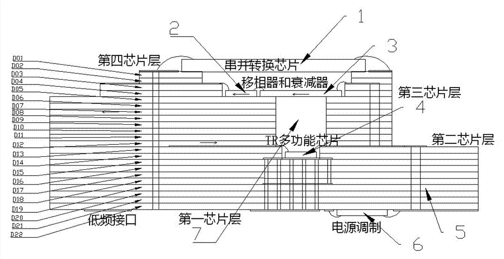
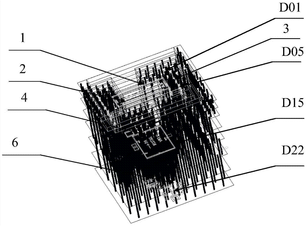
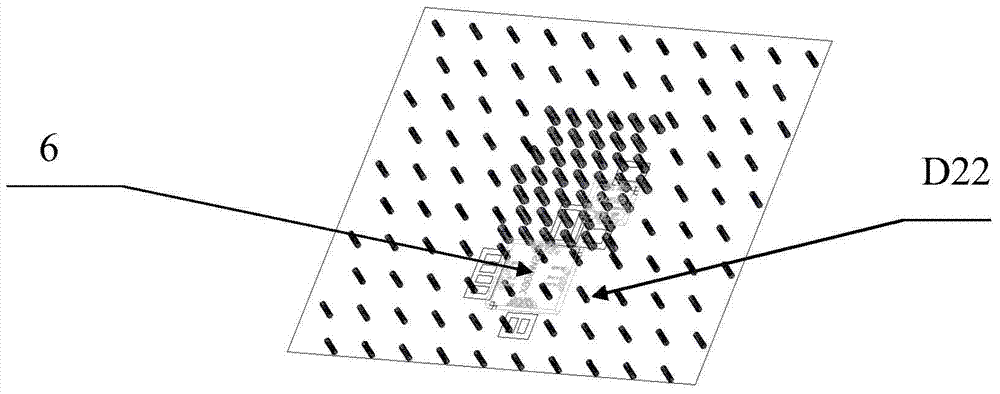
[0026] refer to Figure 1 to Figure 5 . In a best implementation case described below, the T / R component of the millimeter-wave active phased array antenna working in the Ku (14-18GHz) band, the 3D assembly structure of the T / R component chip mainly includes the LTCC substrate, through The serial-to-parallel conversion chip 1, the phase shifter (2), the attenuator 3, the T / R multi-function chip 4 and the power modulator 6 connected together by the transmission line and the vertical interconnection. The large-area metal ground and metal transmission line used for chip bonding in the LTCC substrate used as the chip carrier layer and chip interconnection are all gold layers. The top and bottom surfaces of the LTCC substrate are solderable grounding areas, which are interconnected with the internal grounding metal layer of the LTCC substrate through metallized through holes. The conductive adhesive is used to realize the bonding assembly of the T / R component chip and the LTCC su...


PUM


Abstract

The invention provides a 3D assembling method for integrally integrating chips of T/R assembly, and aims to provide a T/R assembly which has advantages of reliable performance, higher density, more functions, high signal transmission speed, better performance and relatively lower cost. The 3D assembling method is realized through a solution which comprises the steps of performing z-direction expansion on a planar circuit with printed circuit patterns to a green ceramic chip laminate of a three-dimensional circuit through interlayer vertical interconnection; vertically packaging an active device in a rectangular chamber (7) of the green ceramic chip laminate (5), placing a power supply modulator on the back surface of the bottom of the green ceramic chip laminate, and inputting an outer signal from a low-frequency interface at the back surface of the green ceramic chip laminate to a pad of the green ceramic chip laminate (5); performing radio frequency connection among chips through a metal wire bonding vertical interconnection structure among the green ceramic chip laminates, accurately aligning and laminating the green ceramic laminates in a Z direction, and then sintering at a temperature of 900 DEG C, thereby preparing a three-dimensional circuit low-temperature co-sintered ceramic LTCC substrate which is used for high-density circuits with no three-dimensional space interference and is internally provided with a passive element and can be equipped with bare chips or package chips on the surface.

Description

technical field [0001] The invention relates to a 3D integrated assembly method of a T / R component chip in a millimeter wave active phased array antenna. Background technique [0002] In recent years, with the rapid development of communication services, the rapid progress of millimeter-wave monolithic integrated circuits and high-speed digital processing chips has made the application of high-density integrated millimeter-wave active phased array T / R possible. The wide application of my country's on-orbit satellite system and communication data link has higher and higher requirements for the transmission rate and installation space of the phased array T / R components, requiring the phased array T / R components to have higher density, more functions, The requirements of faster signal transmission, better performance, higher reliability, and lower relative cost make the application of millimeter-wave active phased array T / R components very urgent. [0003] In 2008, Yang Guangyu...

Claims


Application Information

Patent Timeline
Patent Type & Authority Applications(China)
IPC IPC(8): H01L21/50
CPCH01L2224/45144H01L2224/48091H01L2224/48227H01L21/76898H01L21/4882H01L21/76895
Inventor 赖复尧赵青李晓艳
Owner 10TH RES INST OF CETC
Why Eureka
Try Eureka