Monolithic silicon-based transmitter

An emitter, silicon-based technology, used in phonon exciters, lasers, laser components, etc., can solve the problems of complex production, CMOS incompatibility, small process tolerance, etc., and achieve simple optical links and high integration. , The effect of large process tolerance

Active Publication Date: 2018-06-19
WUHAN POST & TELECOMM RES INST CO LTD
View PDF3 Cites 6 Cited by
  • Summary
  • Abstract
  • Description
  • Claims
  • Application Information

AI Technical Summary

Problems solved by technology

However, the design structure of these converters is either complicated to manufacture, with small process tolerances, or requires the introduction of high-cost materials in the CMOS process
Both are incompatible with current silicon-dominated CMOS

Method used


Image

  • Monolithic silicon-based transmitter
  • Monolithic silicon-based transmitter
  • Monolithic silicon-based transmitter

Examples


Embodiment Construction

[0030] The present invention will be described in further detail below in conjunction with the accompanying drawings and specific embodiments.

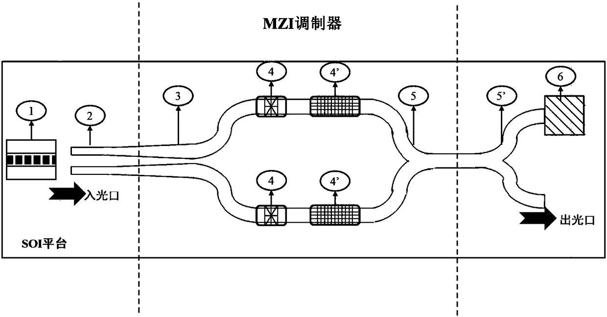
[0031] see figure 1 As shown, the embodiment of the present invention provides a monolithic silicon-based transmitter, which includes: a laser 1 integrated into a silicon-based platform, which is used as an on-chip light source to input continuous laser light; a tip mode formed on the end face of a silicon waveguide A spot matcher 2 is used to match the mode spot of the laser 1; a silicon waveguide biconical beam splitter 3 as the input end of the MZI (Mach-Zehnder interference) modulator is used to split the input optical power (its length design The phase of the waveguide supermode caused by the alignment process error of the laser 1 can be changed, and the light is divided into two paths of equal power and output to the two arms of the MZI modulator); two thermal electrodes 4 and / or are respectively formed on the two arms of the MZ...


PUM


Abstract

The present invention discloses a monolithic silicon-based transmitter, and relates to the silicon photonic and photoelectron integration field. The emitter comprises a laser integrated to a silicon-based platform; a tip mode spot matcher formed on the end face of a silicon waveguide; a silicon waveguide biconical beam splitter used as the input end of an MZI modulator and connected with the tip mode spot matcher; two thermodes respectively formed on the two arms of the MZI modulator and / or two high-frequency electrodes respectively formed on the two arms of the MZI modulator; an MMI beam splitter formed behind the output end of the MZI modulator, wherein two output ports are split by the MMI beam splitter; and a backlight detector formed on the silicon-based platform and connected with one output port of the MMI beam splitter. The monolithic silicon-based transmitter not only realizes the monolithic integration of the laser and the modulator on the silicon-based platform, is low in manufacturing cost, simple in technology and high in integration degree, and facilitates the large-scale production.

Description

technical field [0001] The invention relates to the field of integration of silicon photons and optoelectronics, specifically a monolithic silicon-based emitter. Background technique [0002] With the development of information technology and CMOS (Complementary Metal Oxide Semiconductor, Complementary Metal Oxide Semiconductor) process technology, people require faster and faster computing speed of the system and smaller and smaller chip sizes. However, the chip size of silicon integrated circuits based on traditional etching processes has reached the technological limit; mainly because of the continuous reduction in size, the interconnection delay effect and energy consumption of traditional electrical interconnection-based integrated circuits have gradually emerged. , which limits the improvement of system speed and integration. Compared with the electrical interconnection technology, the optical interconnection technology using photonics as the information carrier has t...

Claims


Application Information

Patent Timeline
Patent Type & Authority Applications(China)
IPC IPC(8): H01S5/026
CPCH01S5/026H01S5/0265
Inventor 冯朋肖希王磊陈代高余少华
Owner WUHAN POST & TELECOMM RES INST CO LTD
Why Eureka
Try Eureka