True blind hole circuit board making process

A manufacturing process and circuit board technology, applied in multi-layer circuit manufacturing, printed circuit manufacturing, printed circuit, etc., can solve the problems that affect the efficiency of operators' production enthusiasm, affect the appearance and exposure of product yield, and the impact of equipment and materials, etc., to achieve It is beneficial to widely promote the application, shorten the production cycle and ensure the effect of product quality

Inactive Publication Date: 2018-06-19
东莞市天晖电子材料科技有限公司
View PDF4 Cites 4 Cited by
  • Summary
  • Abstract
  • Description
  • Claims
  • Application Information

AI Technical Summary

Problems solved by technology

[0003] Since the above process involves copper foil lamination, since the copper foil is relatively soft, it is easy to cause copper foil wrinkle, which affects the appearance and the yield of post-process exposure products; after lamination, it needs to be cured before the next process can be transferred, and the curing takes about 30 minutes. long
Moreover, the coating process has to go through two double-sided coatings. The solvent volatilization during the coating process leads to a poor working environment, and multiple baking is required, which seriously affects the efficiency and production enthusiasm of the operators. In addition, the overall process is various, with curing, coating Processes such as cloth, baking, alignment, exposure, and development are easily affected by equipment and materials, and additional production departments are required, which greatly increases labor costs. It is a labor-intensive and low-efficiency operation method

Method used


Image

  • True blind hole circuit board making process

Examples


Embodiment

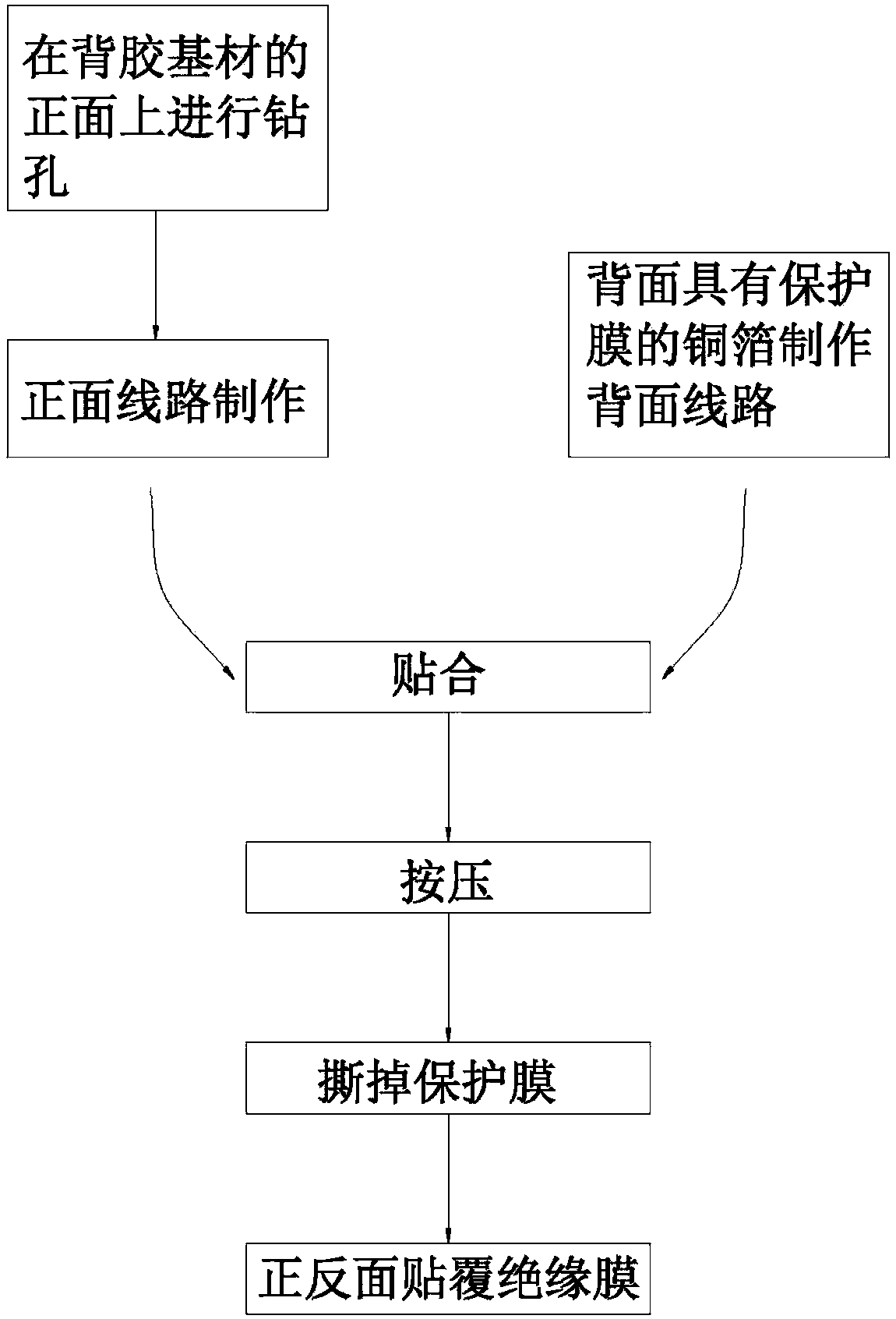
[0021] Example: see figure 1 , a kind of true blind hole circuit board manufacturing process provided by the present embodiment, it comprises the following steps:

[0022] (1) Drill holes on the front side of the adhesive-backed substrate, and then make the front-side circuit; the adhesive-backed substrate is adhesive-backed copper with a thickness of 80-120 microns. Adopt 120 mesh screen printing circuit in the described step (1), the SG of circuit etching cylinder: 1.28-1.32, HCL: 2.0-3.0mol / L, Cu2+: 120~180g / L, temperature 50 ± 2 ℃; Tank concentration 3-5%, temperature 50±2℃;

[0023] (2) The copper foil having a protective film on the back is etched on the back to realize the production of the back circuit; the copper foil is preferably a pure copper foil with a thickness of 18 to 25 microns, and the thickness of the protective film is preferably 55 to 65 microns;

[0024] SG: 1.28-1.32 of the line etching cylinder in the step (2), HCL: 2.0-3.0mol / L, Cu2+: 120~180g / L, te...


PUM


Abstract

The invention discloses a true blind hole circuit board making process. The process comprises steps that (1), drilling on a front side of a gum base material is carried out, and front side circuit making is carried out; (2), back etching of a copper foil having a protection film on the back side is carried out to make a back side circuit; (3), a back side of the gum base material and a front sideof the copper foil are bonded; (4), the gum base material and the copper foil which are bonded are pressed to synthesize a board body; (5), the protection film on the copper foil is torn; and (6), insulation films are pasted on front and back sides of the board body. The process is advantaged in that the process is simple, the circuits at the back and front sides are produced simultaneously, bonding is then carried out, the integral process steps are effectively and integrally simplified, the production period is greatly shortened, production efficiency is improved, manpower and material resources are effectively saved, production cost is reduced, the back side of the copper foil is supported through employing the protection film, the wrinkle rate of the copper foil is effectively reduced,the yield is improved, product quality is guaranteed, and wide popularization and application are facilitated.

Description

technical field [0001] The invention relates to the technical field of circuit board manufacturing technology, in particular to a true blind hole circuit board manufacturing process. Background technique [0002] Printed circuit boards are essential components of various electronic products. Existing printed circuit boards use double-sided copper-clad laminates on the copper foil layer for counter-position exposure and development and then etch to make circuits. The specific process steps are roughly as follows: drilling holes on the front side—attaching the copper foil on the back—pressing and curing - Front and back coating, curing - exposure - development - etching, film fading - front and back insulating layers. [0003] Since the above process involves copper foil lamination, since the copper foil is relatively soft, it is easy to cause copper foil wrinkle, which affects the appearance and the yield of post-process exposure products; after lamination, it needs to be cu...

Claims


Application Information

Patent Timeline
Patent Type & Authority Applications(China)
IPC IPC(8): H05K3/46
CPCH05K3/4611H05K2203/1484
Inventor 郭迎福
Owner 东莞市天晖电子材料科技有限公司
Why Eureka
Try Eureka