Color film substrate, preparation method, display panel and display device
A color film substrate and display panel technology, applied in nonlinear optics, instruments, optics, etc., can solve problems such as abnormal display in the display area, affecting product quality, abnormal panel display, etc., to solve the problem of abnormal display, improve display effect, The effect of increased contact area
- Summary
- Abstract
- Description
- Claims
- Application Information
AI Technical Summary
Problems solved by technology
Method used
Image
Examples
Embodiment 1
[0029] Depend on figure 1 It can be seen that the color filter substrate described in this application includes a base substrate 1 and a black matrix layer 2 disposed on one side of the base substrate 1; the side of the black matrix layer 2 away from the base substrate 1 is provided with a peripheral Columnar spacers 3, that is, peripheral columnar spacers 3 are arranged on the side of the color filter substrate facing the array substrate; the peripheral columnar spacers 3 are arranged correspondingly to the sealant coating area of the color filter substrate , used to make the color filter substrate sealed and connected to the array substrate through the peripheral columnar spacer 3 and the sealant; the peripheral columnar spacer 3 and the surface of the black matrix layer 2 are both provided with an ITO layer 4, And make the ITO layer 4 contact with the ends of the peripheral column spacers 3 and the black matrix layer 2 at the same time. In this way, when the color filter...
Embodiment 2
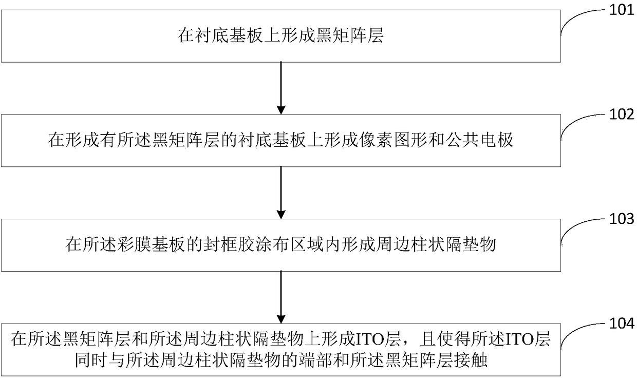
[0037] refer to figure 2 Shown is a flowchart of an embodiment of the method for preparing a color filter substrate provided by the present invention. The preparation method of the color filter substrate includes:
[0038] Step 101, forming a black matrix layer on a base substrate; wherein, the base substrate may be a glass substrate; the process of forming the black matrix layer also includes forming a required black matrix pattern structure through a patterning process.
[0039] Step 102, forming pixel patterns and common electrodes on the base substrate on which the black matrix layer is formed;
[0040] Step 103, forming peripheral columnar spacers in the frame sealant coating area of the color filter substrate; wherein, the peripheral columnar spacers and the main columnar spacers can be prepared through the same mask process, so that no additional mask craft.
[0041] Step 104 , forming an ITO layer on the black matrix layer and the peripheral column spacers, and m...
Embodiment 3
[0044] refer to image 3 Shown is a schematic structural diagram of an embodiment of the display panel provided by the present invention. The display panel includes an array substrate and any one of the color filter substrates described above. It can be seen from the figure that metal wires 7 are arranged in the coating area of the sealant 8 of the array substrate 6; the ITO layer 4 is in contact with the metal wires 7, so that the black matrix layer 2 is connected to the The metal wires 7 are electrically connected, so that when the potential in the metal wires is zero, the charges in the black matrix layer 2 can be released. In addition, in the display area, RGB sub-pixels (11, 12, 13) and main column spacers are also arranged on the color filter substrate.
[0045] refer to Figure 4 As shown in FIG. 2 , it is a schematic structural diagram of the sealant region of the display panel in the prior art. Figure 4 Designed for common panel-to-box structures. The BM adopt...
PUM
 Abstract
Description
Claims
Application Information


