Superjunction IGBT with enhanced carrier storage effect
A technology of gate structure and conductivity type, applied in the field of power semiconductor devices, can solve the problems of increasing on-voltage drop, increasing on-state power consumption, weak storage effect, etc.
- Summary
- Abstract
- Description
- Claims
- Application Information
AI Technical Summary
Problems solved by technology
Method used
Image

Examples
Embodiment Construction
[0058] The present invention will be described in detail below in conjunction with the accompanying drawings.
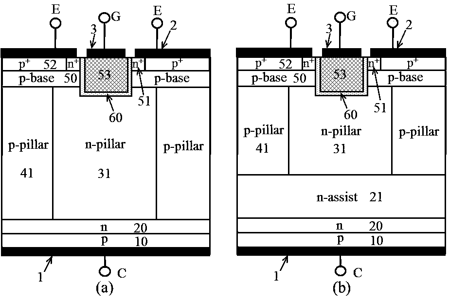
[0059] figure 1 (a) shows the schematic diagram of the traditional super-junction IGBT structure, figure 1 (b) shows the schematic diagram of the traditional semi-superjunction IGBT structure. Compared with the super-junction IGBT, the semi-super-junction IGBT has one more bearing part between the n-pillar area (n-pillar area 31) and the p-pillar area (p-pillar area 41) and the buffer zone (n area 20). An auxiliary layer (n-assist region 21 ) for applying a voltage, wherein the doping concentration of the auxiliary layer may be lower than or equal to the doping concentration of the n-pillar region (n-pillar region 31 ). When a gate voltage exceeding the threshold voltage is applied to the gate (G), the surface of the base region (p-base region 50) under the gate dielectric (60) is inversion, forming an electron channel, and this electron channel will emit the regio...
PUM
 Abstract
Description
Claims
Application Information
 - R&D
- Intellectual Property
- Life Sciences
- Materials
- Tech Scout
- Unparalleled Data Quality
- Higher Quality Content
- 60% Fewer Hallucinations
Browse by: Latest US Patents, China's latest patents, Technical Efficacy Thesaurus, Application Domain, Technology Topic, Popular Technical Reports.
© 2025 PatSnap. All rights reserved.Legal|Privacy policy|Modern Slavery Act Transparency Statement|Sitemap|About US| Contact US: help@patsnap.com