Metal-insulator-semiconductor (MIS) grid enhanced high electron mobility transistor (HEMT) device based on gallium nitride (GaN) and manufacture method of MIS grid enhanced HEMT device

An enhanced device technology, applied in the field of microelectronics, can solve the problems of low device reliability, high current density coexistence, device performance and reliability effects, etc., and achieve the effect of eliminating polarization effects and good enhanced characteristics

Active Publication Date: 2012-08-08
云南凝慧电子科技有限公司
View PDF3 Cites 30 Cited by
  • Summary
  • Abstract
  • Description
  • Claims
  • Application Information

AI Technical Summary

Problems solved by technology

[0011] First, the increase of threshold voltage is often at the expense of reducing the current density, and it is difficult to achieve the coexistence of high threshold voltage and high current density;
[0012] Second, whether etching to form trench gates or fluorine ion implantation will cause damage to the material, although a certain amount of dam

Method used


Image

  • Metal-insulator-semiconductor (MIS) grid enhanced high electron mobility transistor (HEMT) device based on gallium nitride (GaN) and manufacture method of MIS grid enhanced HEMT device
  • Metal-insulator-semiconductor (MIS) grid enhanced high electron mobility transistor (HEMT) device based on gallium nitride (GaN) and manufacture method of MIS grid enhanced HEMT device
  • Metal-insulator-semiconductor (MIS) grid enhanced high electron mobility transistor (HEMT) device based on gallium nitride (GaN) and manufacture method of MIS grid enhanced HEMT device

Examples


Embodiment 1

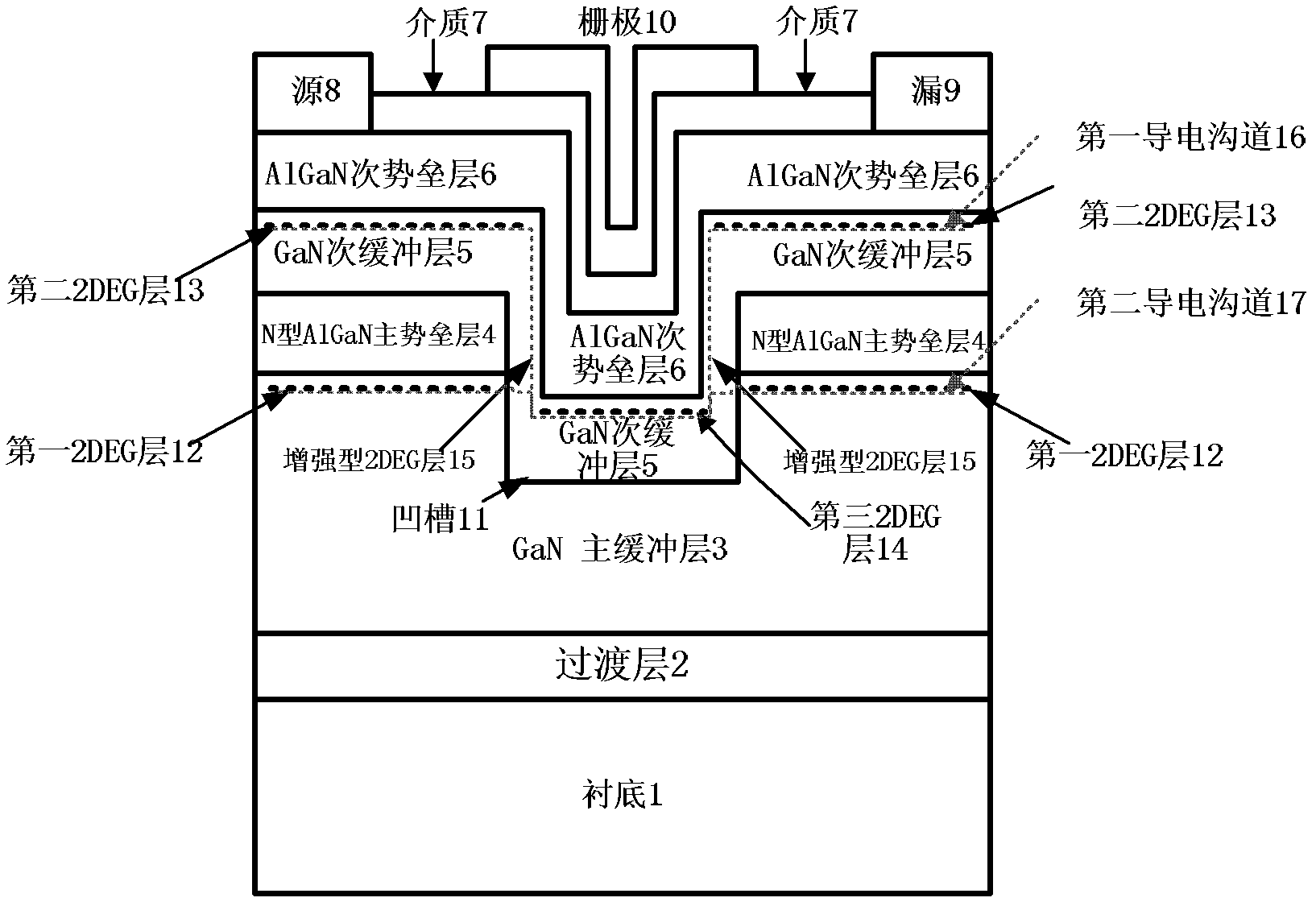
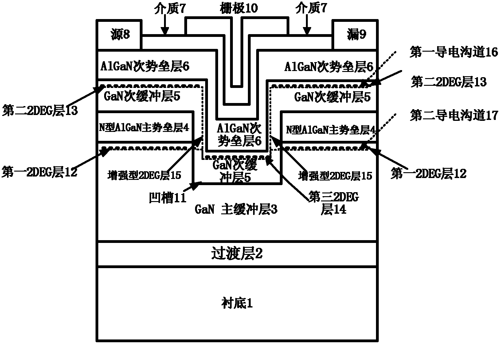
[0048] The substrate is made of sapphire, the transition layer is AlN, the thickness of the GaN main buffer layer is 1.5um, and the thickness of the Al 0.35 Ga 0.65 The thickness of the N main barrier layer is 16nm, the groove etching depth is 40nm, the thickness of the GaN sub-buffer layer is 20nm, Al 0.35 Ga 0.65 The GaN-based MIS gate-enhanced HEMT device with an N-time barrier layer thickness of 16nm and a gate dielectric layer thickness of 2nm is as follows:

[0049] Step 1, place the C-plane sapphire substrate in the metal organic chemical vapor deposition MOCVD reaction chamber, and evacuate the vacuum degree of the reaction chamber to 1×10 -2 Under Torr, heat treatment and surface nitriding of the sapphire substrate are carried out under the protection of a mixture of hydrogen with a flow rate of 1500 sccm and ammonia gas with a flow rate of 2000 sccm, with a heating temperature of 1050° C. and a pressure of 20 Torr.

[0050] Step 2, using MOCVD technology, under th...

Embodiment 2

[0071] The substrate is made of silicon carbide SiC, the transition layer is AlN, the thickness of the GaN main buffer layer is 2.5um, and the Al 0.27 Ga 0.73 The thickness of the N main barrier layer is 24nm, the groove etching depth is 90nm, the thickness of the GaN sub-buffer layer is 60nm, Al 0.27 Ga 0.73 The GaN-based MIS gate-enhanced HEMT device with an N-time barrier layer thickness of 24nm and a gate dielectric layer thickness of 8nm is as follows:

[0072] Step 1, place the silicon carbide SiC substrate in the MOCVD reaction chamber for heat treatment and surface nitriding. The process conditions are: the vacuum degree of the reaction chamber is 1×10 -2 Under Torr, the hydrogen flow rate is 1500 sccm, the ammonia gas flow rate is 3500 sccm, the heating temperature is 950° C., and the pressure is 40 Torr.

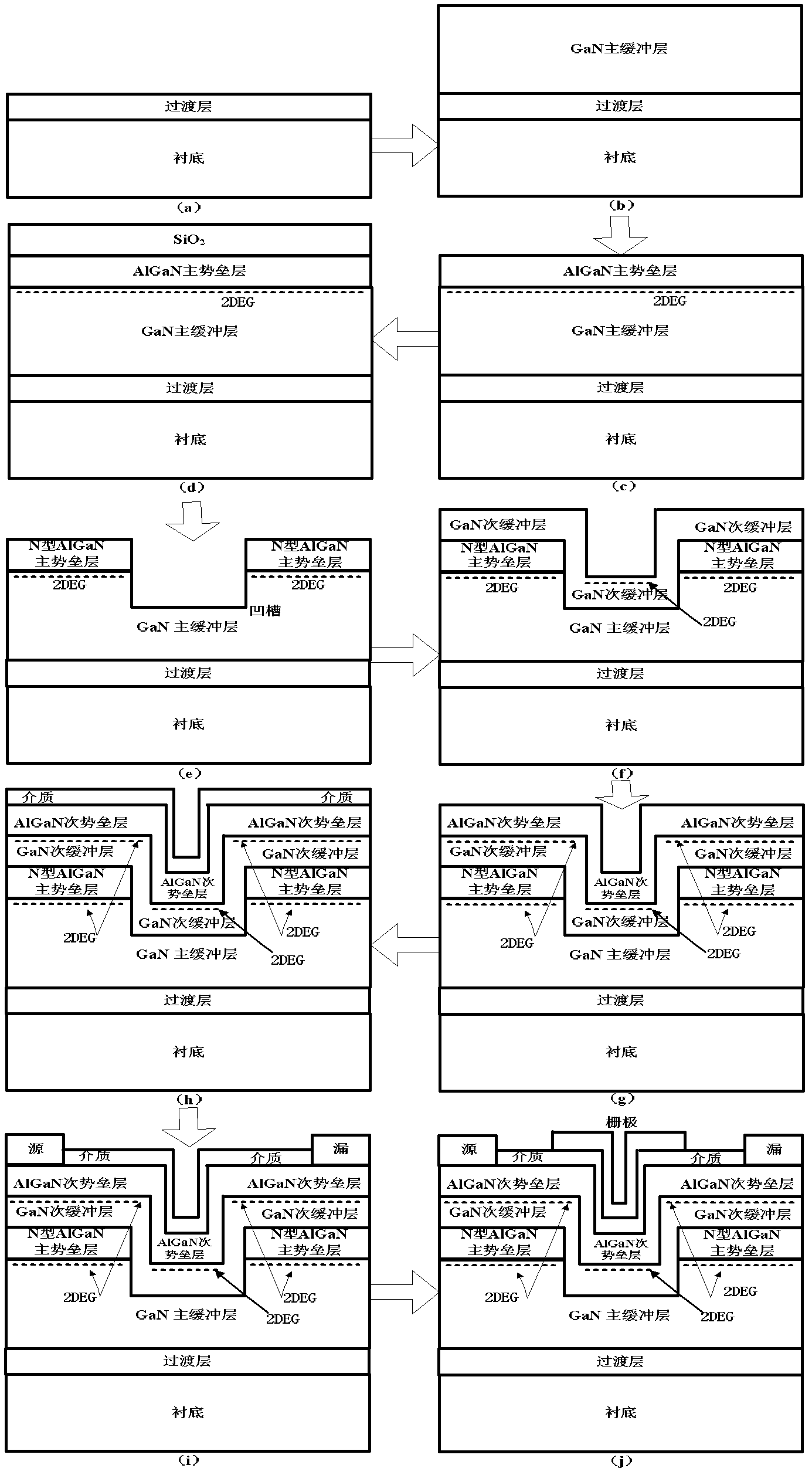
[0073] Step 2, using MOCVD technology, epitaxial AlN transition layer with a thickness of 150nm on the silicon carbide SiC substrate, such as figure 2 (a), th...

Embodiment 3

[0094] The substrate is made of sapphire, the transition layer is AlN, the thickness of the GaN main buffer layer is 3.5um, and the thickness of the Al 0.2 Ga 0.8 The thickness of the N main barrier layer is 36nm, the groove etching depth is 140nm, the thickness of the GaN sub-buffer layer is 100nm, Al 0.2 Ga 0.8 The GaN-based MIS gate-enhanced HEMT device with the thickness of the N-time barrier layer being 36nm and the thickness of the gate dielectric layer being 15nm, the steps are:

[0095] Step A, place the sapphire substrate in the metal organic chemical vapor deposition MOCVD reaction chamber, conduct heat treatment and surface nitriding on the sapphire substrate under the protection of the mixed gas of ammonia and hydrogen, and pump the vacuum degree of the reaction chamber to 1× 10 -2 Under Torr, the flow rate of hydrogen gas is 1500 sccm, the flow rate of ammonia gas is 2000 sccm, the heating temperature is 1050° C., and the pressure is 20 Torr.

[0096] Step B, ...


PUM

PropertyMeasurementUnit
Doping concentrationaaaaaaaaaa
Depthaaaaaaaaaa
Thicknessaaaaaaaaaa

Abstract

The invention discloses a metal-insulator-semiconductor (MIS) grid enhanced high electron mobility transistor (HEMT) device based on gallium nitride (GaN) and a manufacture method of the MIS grid enhanced HEMT device and mainly solves the problems that the current density and the reliability of the existing GaN base enhanced device are low. The device is structurally characterized in that a transition layer (2) and a GaN main buffer layer (3) are sequentially arranged on a substrate (1), the middle of the GaN main buffer layer (3) is provided with a groove (11), an AlGaN main barrier layer (4) is arranged above the GaN main buffer layer arranged at two sides of the groove, a GaN sub buffer layer (5) and an AlGaN sub barrier layer (6) are sequentially arranged on the surface of the AlGaN main barrier layer (4) arranged above the groove inner wall and the two sides of the groove, the two sides of the top end of the AlGaN sub barrier layer (6) are respectively a source electrode (8) and a drain electrode (9), a medium layer (7) is arranged outside the source electrode and the drain electrode, a grid electrode (10) is arranged on the medium layer (7) and covers the whole groove region, and the mature flow process is adopted for the whole device manufacture. The MIS grid enhanced HEMT device has the advantages that the enhanced type characteristics are good, the current density is high, the breakdown voltage is high, and the device reliability is high. The MIS grid enhanced HEMT device can be used in high-temperature high-frequency high-power devices, high-power switches and digital circuits.

Description

technical field [0001] The invention belongs to the technical field of microelectronics, and relates to a semiconductor device and a manufacturing process, in particular to a metal insulator semiconductor MIS gate-enhanced high electron mobility transistor HEMT device and a manufacturing method based on a GaN material, which can be used for high-temperature, high-frequency, high-power applications as well as high power switching and digital circuits. Background technique [0002] GaN is a new type of wide band gap compound semiconductor material, which has excellent characteristics that many silicon-based semiconductor materials do not have, such as a wide band gap of 3.14eV, up to 3×10 6 V / cm breakdown electric field, high thermal conductivity, corrosion resistance and radiation resistance. More importantly, GaN materials can form AlGaN / GaN heterojunction structures, which can obtain higher than 1500cm 2 / Vs electron mobility, and up to 3×10 7 cm / s saturation electron ve...

Claims


Application Information

Patent Timeline
IPC IPC(8): H01L29/778H01L29/06H01L21/336
CPCH01L29/4236H01L29/2003H01L29/66462H01L29/7789
Inventor 张进成张琳霞郝跃马晓华王冲霍晶艾姗党李莎孟凡娜姜腾赵胜雷
Owner 云南凝慧电子科技有限公司
Why Eureka
Try Eureka