misfet

a technology of misfet and insulating material, which is applied in the direction of semiconductor devices, semiconductor/solid-state device details, electrical apparatus, etc., can solve the problems of increasing the number of processing steps, increasing the current, and increasing the complexity of the overall process technology, so as to improve the manufacturing process of misfet.

Inactive Publication Date: 2005-04-07
QUANTUM SEMICON
View PDF8 Cites 29 Cited by
  • Summary
  • Abstract
  • Description
  • Claims
  • Application Information

AI Technical Summary

Benefits of technology

[0024] It is an object of the present invention

Problems solved by technology

For deep sub-micron CMOS, as the gate lengths get shorter, leakage current tends to get higher, and the overall process technology becomes more complex.
Not only the number of processing steps increases, but the complexity and difficulty of some of those steps is also increased.
The limitations to make Vertical MOSFETs with very short channel lengths will no longer be technological, but related to device physics.
With horizontal MOSFETs, it is also possible to introduce asymmetry, but that comes at a cost in terms of process complexity (extra masks to differentiate source from drain for each type of device).
And in any case, the doping and/or heterojunction profiles (made by ion implantation) can never come close to what low temperature epitaxy has demonstrated.
Naturally, the necessity of applying drain bias, leads to even stronger scaling

Method used


Image

  • misfet
  • misfet
  • misfet

Examples


Embodiment Construction

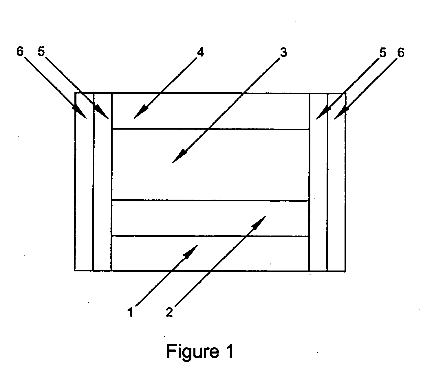
[0058] In FIG. 1, showing a schematic cross section of the device, the following layers may be distinguished: [0059] Layer 1 is the contact to the Source: metal with work-function or Fermi-Level in the middle of the band-gap of the Source material. [0060] Layer 2 is the Source: “narrow” band-gap material, with its mid-gap point aligned with the mid-gap point of the channel material, resulting in similar offsets in the conduction and valence bands, with respect to the channel material. [0061] Layer 3 is the channel: “wide” band-gap material. [0062] Layer 4 is the Drain: metal with a work-function or Fermi-Level in the middle of the gap of the channel material. [0063] Layer 5 is the Gate insulator. [0064] Layer 6 is the Gate electrode: conductor with Fermi-Level in the middle of the gap of the channel material. [0065] Layers 1, 4, and 6, can be of the same material.

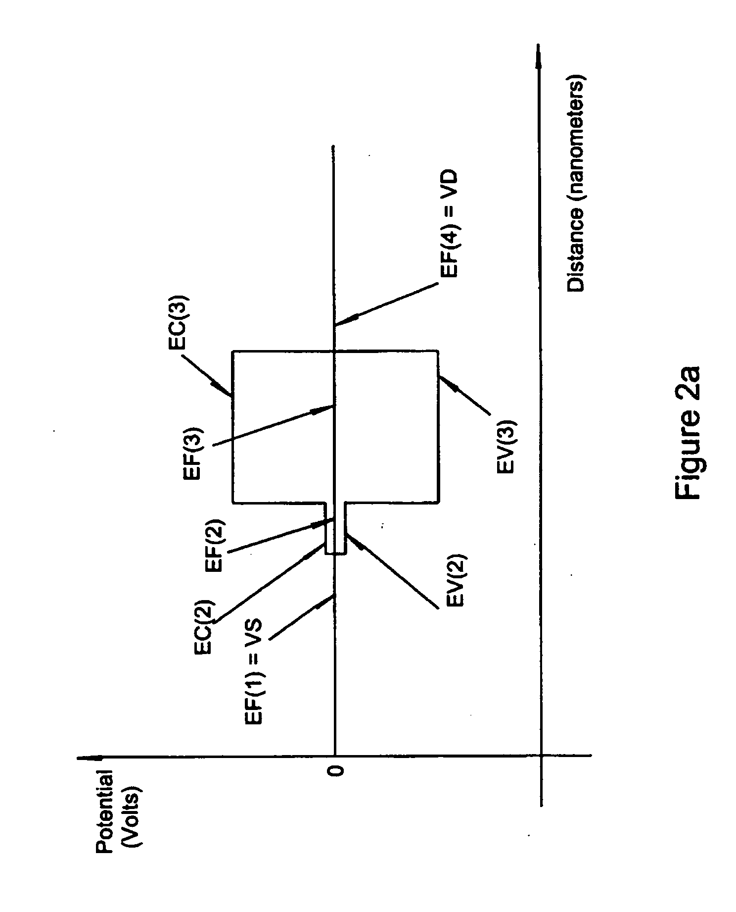
[0066] In FIG. 2a, a band diagram of the device is shown when no voltage is applied, in other words the drain to source ...


PUM


Abstract

A metal insulator semiconductor field effect transistor (MISFET) is disclosed comprising a source layer being made with a material having a source band-gap (EG2) and a source mid-gap value (EGM2), the source layer having a source Fermi-Level (EF2). A drain layer has a drain Fermi-Level (EF4). A channel layer is provided between the source layer and the drain layer, the channel layer being made with a material having a channel band-gap (EG3) and a channel mid-gap value (EGM3), the channel layer having a channel Fermi-Level (EF3). A source contact layer is connected to the source layer opposite the channel layer, the source contact layer having a source contact Fermi-Level (EF1). A gate electrode has a gate electrode Fermi-Level (EF6). The source band-gap is substantially narrower (EG2) than the channel band-gap (EG3). The source contact Fermi-Level (EF1), the source Fermi-Level (EF2), the channel Fermi-Level (EF3), the drain Fermi-Level (EF4) and the gate electrode Fermi-Level (EF6) are equal to the source mid-gap value (EGM2) and the channel mid-gap value (EGM3), within a predetermined tolerance value, when no voltage is applied to the device.

Description

[0001] This is a continuation-in-part of U.S. application Ser. No. 09 / 889,815, filed Jul. 20, 2001, U.S. Pat. No. ______, which was the National Stage of International Application No. PCT / IB00 / 00235 (WO0051165), filed Feb. 24, 2000, which claimed the benefit of U.S. Provisional Application No. 60 / 121,473 filed Feb. 24, 1999, each of which is incorporated herein by reference in its entirety.FIELD OF THE INVENTION [0002] The field of the invention is metal insulator semiconductor field effect transistors (MISFETs). BACKGROUND OF THE INVENTION [0003] Complementary Metal-Oxide Semiconductor (CMOS) has been the semiconductor technology of choice since the late 1970's, and in 1998 the 0.25 micron CMOS technology generation is in production. There are many reasons to choose CMOS over other technologies. The most important is the reduced power consumption, because the basic building block of circuits for binary logic, the CMOS “Inverter”, only consumes power when changing logic states. [000...

Claims


Application Information

Patent Timeline
IPC IPC(8): H01L21/336H01L21/8238H01L27/092H01L29/08H01L29/165H01L29/45H01L29/78H01L29/786
CPCH01L21/823885H01L27/092H01L29/0895H01L29/165H01L29/78642H01L29/66643H01L29/66666H01L29/7827H01L29/7839H01L29/456
Inventor AUGUSTO, CARLOS
Owner QUANTUM SEMICON
Why Eureka
Try Eureka