Photo-responsive organic field effect transistor

a photo-responsive, organic field effect technology, applied in the field of transistors, can solve the problems of large drain current, rugged and lightweight, and mechanical flexibility

Inactive Publication Date: 2006-01-31
JAWAHARLAL NEHRU CENT FOR ADVANCED SCI RES
View PDF30 Cites 27 Cited by
  • Summary
  • Abstract
  • Description
  • Claims
  • Application Information

AI Technical Summary

Problems solved by technology

Their switching properties are similar to typical thin film transistors manufactured from silicon and through conventional fabrication methods, but they are mechanically flexible, rugged and lightweight.
Positive charges of the remaining holes bias the source-channel junction forward, leading to large drain current.

Method used


Image

  • Photo-responsive organic field effect transistor
  • Photo-responsive organic field effect transistor
  • Photo-responsive organic field effect transistor

Examples


example

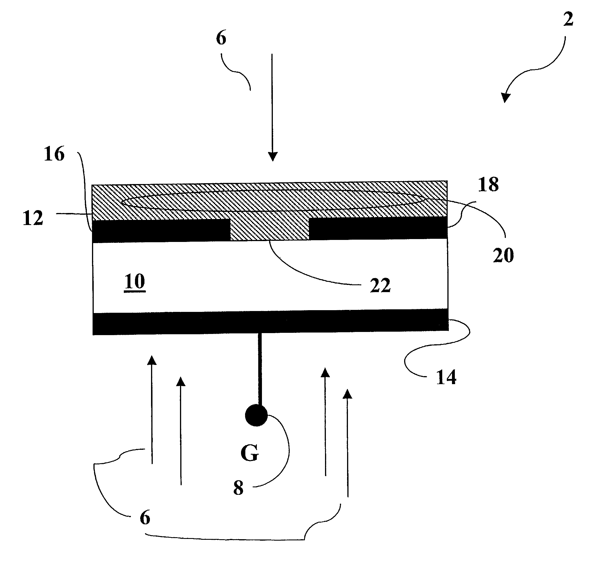
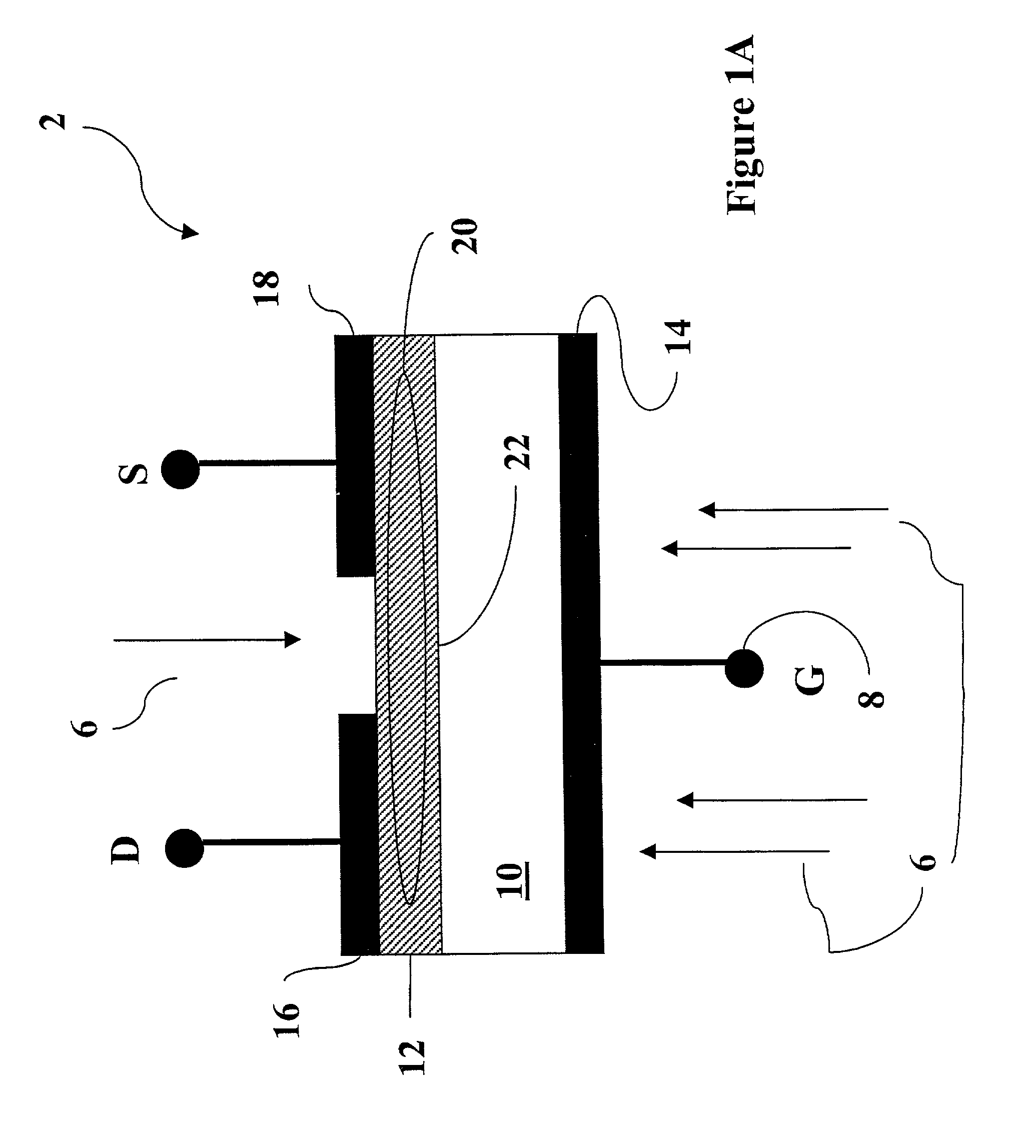
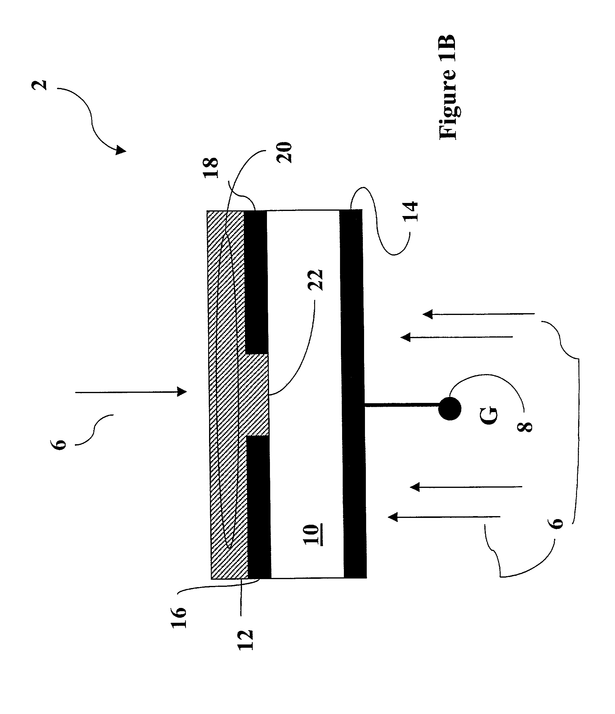
[0038]A FET 2 with P3OT comprising the semiconducting-photoconducting layer 12 and PVA comprising the insulating layer 10 was fabricated. PVA, which is soluble in warm water (50° C.) and transparent, was cast on a glass substrate coated with a partially transparent (10%) gate aluminum electrode 14 to form a uniform layer. The insulating layer coated on the substrate was thoroughly dried. Regioregular Poly (3-octylthiophene), P3OT, and Poly (3-hexylthiophene) with a 98.5% head to tail regiospecific conformation was obtained commercially from Aldrich Inc., USA and used as received. P3OT was dissolved in chloroform and spin coated on the insulator layer 10 to yield a 100 nm thick layer 12. Uniform bilayer of the polymers with a sharp interface 22 was possible partly due to different solvents. Gold electrodes, 3 mm wide with an inter-electrode spacing of 70 microns, forming the channel length, was deposited on the P3OT layer 12 to form the source electrode 18 and drain electrode 16. The...


PUM

PropertyMeasurementUnit
dielectric constantaaaaaaaaaa
drain currentaaaaaaaaaa
relative dielectric constantaaaaaaaaaa

Abstract

A polymer-based field effect transistor photosensitive to incident light, which may enhance the transistor's characteristics and controlling parameters of the transistor state. The transistor is comprised of a metal-insulator-semiconductor structure with the insulating and semiconducting layers made of a polymeric media. The semiconducting polymer which also is photoconducting, forms the charge transport layer between the source and drain. The transistor exhibits large photosensitivity indicated by the sizable changes in the drain-source current, by a factor of 100–1000 even at low levels of light with illumination of approximately 1 mlux. The photosensitivity of the transistor is further enhanced with introduction of dilute quantity electron acceptor moieties in the semiconducting polymer matrix. Several applications of the light-responsive polymer-transistor are disclosed, such as use as a logic element and as a backbone of an image sensor.

Description

[0001]The present application claims the benefit of priority of U.S. Provisional Application No. 60 / 259,375, filed Jan. 2, 2001, the contents of which are herein incorporated by reference in their entirety.FIELD OF THE INVENTION[0002]The instant invention is related generally to the field of transistors. More specifically, the present invention related to transistors based on semiconducting polymers and the use and manufacture of said transistors.BACKGROUND OF THE INVENTION[0003]Classical MIS structure field-effect transistors, commonly called MISFETs or MOSFETs, are generally formed on a silicon substrate strongly doped to make the transistors conduct. A metal layer is deposited on one surface of the substrate so that the grid voltage can be applied. An insulating silica layer is grown on the other surface of the substrate. A semiconducting layer and the two metal contacts constituting the source and drain are applied to this silica layer. The source and drain may be in contact wit...

Claims


Application Information

Patent Timeline
Patent Type & Authority Patents(United States)
IPC IPC(8): H01L51/00H01L21/00H01L51/05H01L51/30H01L51/42
CPCB82Y10/00H01L51/428H01L51/0036H01L51/004H01L51/0046H01L51/005Y02E10/549H01L51/0545H01L51/4226H01L51/4253H01L51/0516H10K85/141H10K85/211H10K85/113H10K85/60H10K10/468H10K10/466H10K30/151H10K30/65H10K30/30
Inventor NARAYAN, KAVASSERY SURESWARAN
Owner JAWAHARLAL NEHRU CENT FOR ADVANCED SCI RES
Why Eureka
Try Eureka