Image sensor and forming method thereof

An image sensor and photosensitive area technology, applied in the direction of electric solid-state devices, semiconductor devices, electrical components, etc., can solve the problems of large dark current and poor image quality, and achieve the effect of reducing white pixels, reducing dark current, and reducing optical crosstalk

Inactive Publication Date: 2018-06-29
HUAIAN IMAGING DEVICE MFGR CORP
View PDF6 Cites 9 Cited by
  • Summary
  • Abstract
  • Description
  • Claims
  • Application Information

AI Technical Summary

Problems solved by technology

[0006] However, the existing CMOS image sensors have the disadvantages of large dark current and poor image quality

Method used


Image

  • Image sensor and forming method thereof
  • Image sensor and forming method thereof
  • Image sensor and forming method thereof

Examples


Embodiment Construction

[0025] There are many problems in the image sensor, for example, the dark current of the image sensor is relatively large.

[0026] Now in conjunction with a CMOS image sensor, analyze the reason why the dark current of the CMOS image sensor is relatively large:

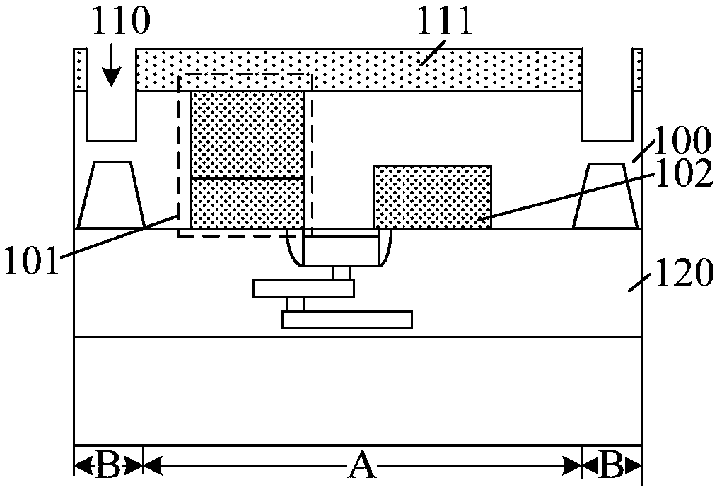
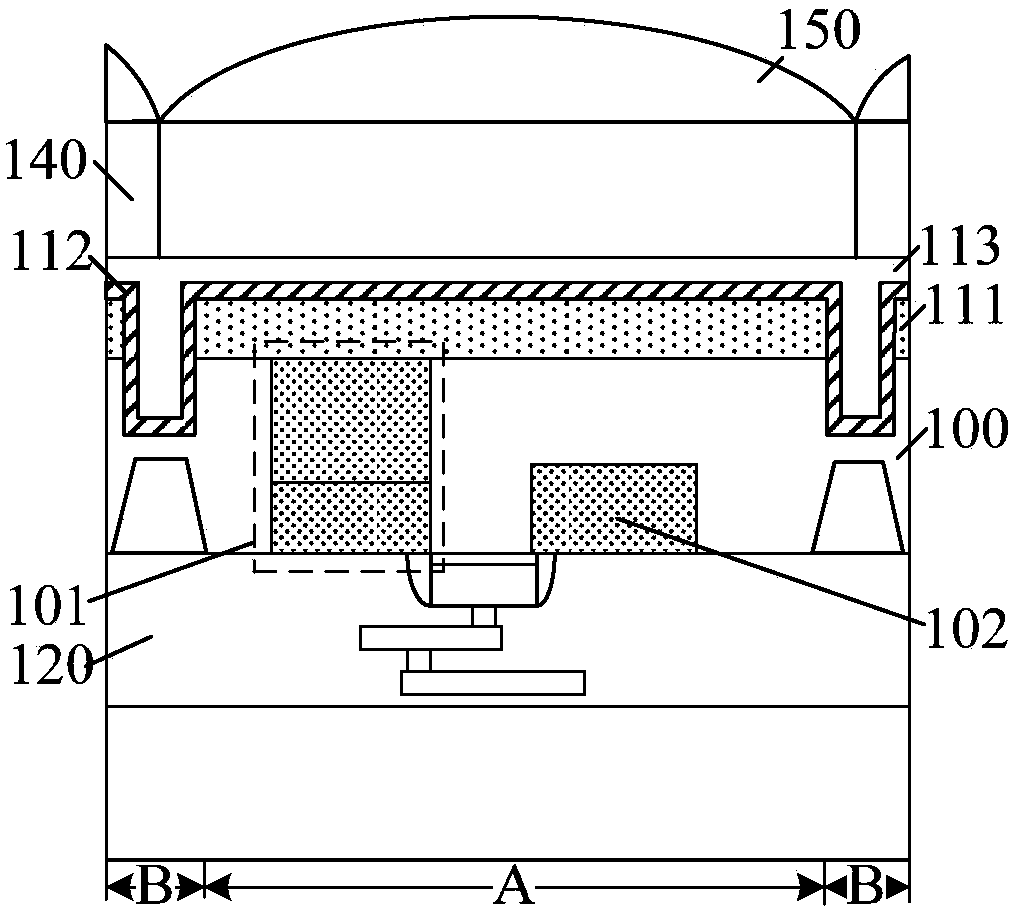
[0027] figure 1 with figure 2 It is a structural schematic diagram of each step of a method for forming a CMOS image sensor.

[0028] Please refer to figure 1 , the CMOS image sensor includes: a substrate 100, the substrate 100 includes an opposite first surface and a second surface, the substrate includes a plurality of discrete photosensitive regions A and adjacent photosensitive regions A In the isolation region B, the first surface of the photosensitive region A of the substrate 100 has a gate structure; the photosensitive region A on both sides of the gate structure has a photodiode 101 and a diffusion region 102 in the substrate 100, and the first The face surface has a dielectric layer 120 covering the ga...


PUM


Abstract

The invention provides an image sensor and a forming method thereof. The forming method of the image sensor comprises the steps that a substrate is provided, wherein the substrate comprises a first surface and a second surface which are opposite to each other, the substrate also comprises a plurality of separated light sensing regions and isolation regions between the adjacent light sensing regions, a light sensing element is arranged in the position, in each light sensing region, in the substrate, and the second surface is exposed out of the light sensing elements; grooves are formed in the positions, in the isolation regions, in the substrate; the first surface is exposed out of the grooves; doping treatment is conducted on the bottoms and the side walls of the grooves, and doping regions are formed in the positions, at the bottoms and side walls of the grooves, in the substrate; after the doping regions are formed, isolation structures are formed in the grooves. The dark current ofthe image sensor formed through the method is small.

Description

technical field [0001] The invention relates to the technical field of semiconductor manufacturing, in particular to an image sensor and a forming method thereof. Background technique [0002] With the continuous improvement of semiconductor technology, the image sensor (Image Sensor), as a basic device for information acquisition, has been more and more widely used in modern society. [0003] According to different components, the image sensor can be divided into two categories: CCD (Charge Coupled Device, Charge Coupled Device) image sensor and CMOS (Complementary Metal-Oxide Semiconductor, metal oxide semiconductor element) image sensor. With the development of semiconductor technology, the performance of CMOS transistors has gradually improved, and the resolution has gradually surpassed that of CCD image sensors. The CMOS image sensor has the characteristics of high integration, low power consumption, high speed, and low cost. [0004] CMOS image sensor is a typical so...

Claims


Application Information

Patent Timeline
Patent Type & Authority Applications(China)
IPC IPC(8): H01L27/146
CPCH01L27/1463H01L27/1464H01L27/14683
Inventor 穆钰平周艮梅黄晓橹陈世杰吕相南
Owner HUAIAN IMAGING DEVICE MFGR CORP
Why Eureka
Try Eureka