Preparation of array type TiO2/CdS composite electron transport layer and bulk heterojunction solar cell application of array type TiO2/CdS composite electron transport layer

An electron transport layer and solar cell technology, applied in the field of solar cells, achieves the effects of good application prospects, inhibition of charge recombination, and low cost

Pending Publication Date: 2022-04-01
HEFEI UNIV OF TECH
View PDF0 Cites 0 Cited by
  • Summary
  • Abstract
  • Description
  • Claims
  • Application Information

AI Technical Summary

Problems solved by technology

The ideal one-dimensional CdS nanorod structure needs to grow vertically and have a suitable aspect ratio; it is challenging to grow high-quality CdS nanorods on the FTO conductive substrate with high roughness

Method used


Image

  • Preparation of array type TiO2/CdS composite electron transport layer and bulk heterojunction solar cell application of array type TiO2/CdS composite electron transport layer
  • Preparation of array type TiO2/CdS composite electron transport layer and bulk heterojunction solar cell application of array type TiO2/CdS composite electron transport layer
  • Preparation of array type TiO2/CdS composite electron transport layer and bulk heterojunction solar cell application of array type TiO2/CdS composite electron transport layer

Examples


Embodiment 1

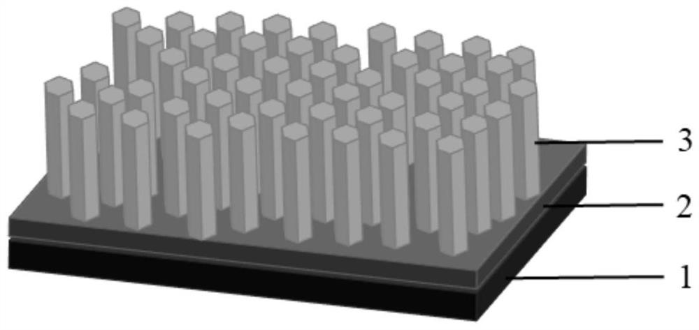
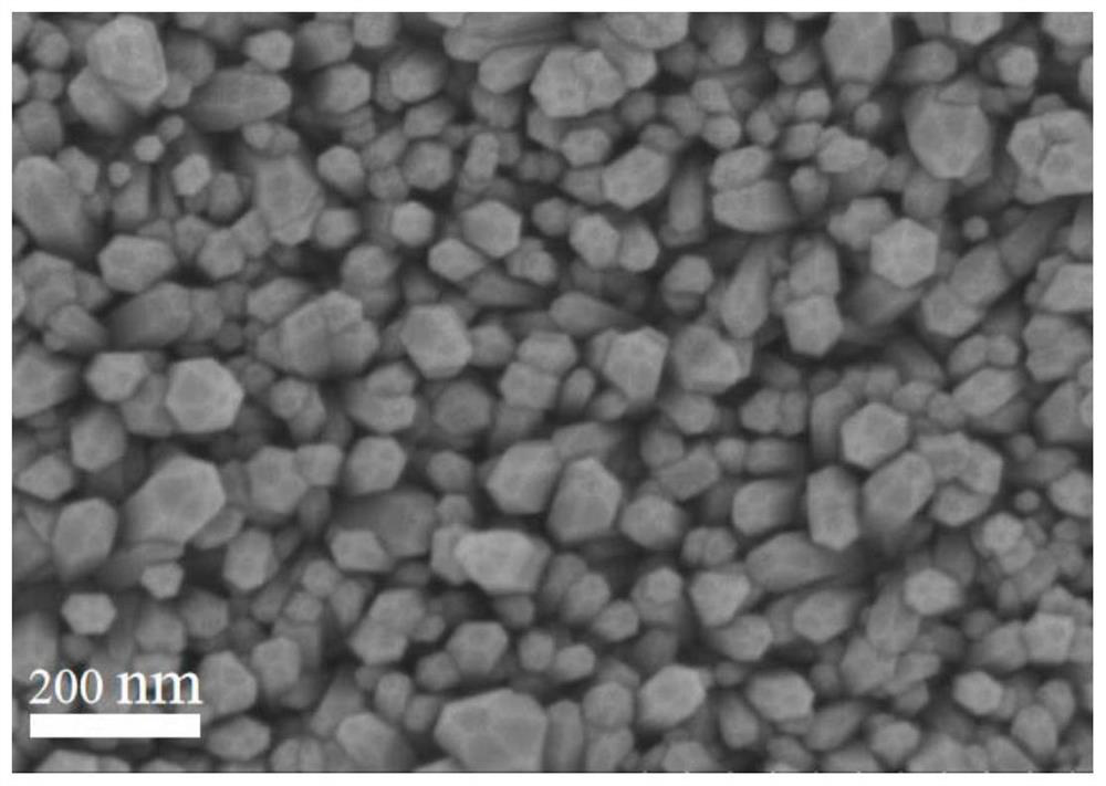
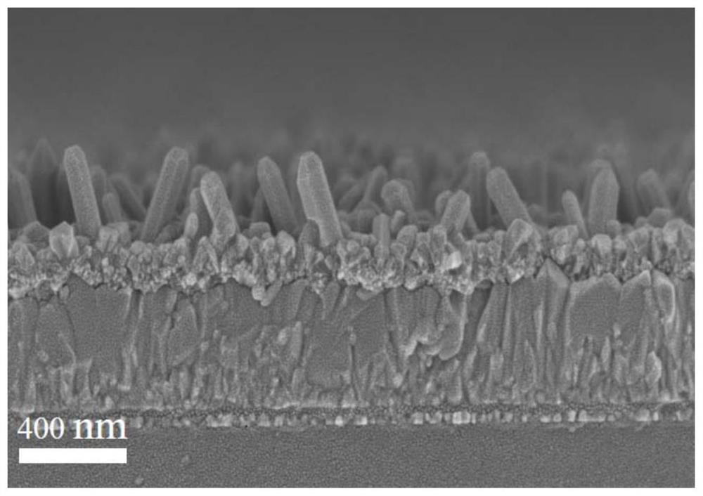
[0045] Preparation of array-based TiO 2 / CdS composite nanostructure electron transport layer perovskite solar cell, the specific steps are as follows:

[0046] 1. Use standard deionized water, IPA and PA to ultrasonically clean the etched FTO glass for 15 minutes, then immediately dry it with a nitrogen gun and then perform UVO treatment for 20 minutes;

[0047] 2. Take 80 μL of TiO 2 The precursor solution was added dropwise onto the FTO, and spin-coated at a speed of 500rpm for 3s, and then spin-coated at a speed of 2000rpm for 30s. After the spin-coating, it was annealed on a heating table at 135°C for 10min, and finally placed in a muffle furnace. Sinter at 500°C for 30 minutes to form a dense layer;

[0048] 3. Mix 0.01M Cd(NO 3 ) 2 4H 2 O, 0.03M thiourea and 0.006M glutathione (GSH) were sequentially added to 80 mL of deionized water, and stirred at room temperature for 15 min;

[0049] 4. Will contain TiO 2 The FTO of the dense layer was immersed in the solution...

Embodiment 2

[0055] Unlike Example 1, the hydrothermal heat in step 4 is 90min, and the prepared MAPbI 3 The perovskite solar cell has an efficiency of 18.72%.

Embodiment 3

[0057] Different from Example 1, the hydrothermal heat in step 4 is 100min, and the prepared MAPbI 3 The perovskite solar cell has an efficiency of 19.01%.


PUM

PropertyMeasurementUnit
thicknessaaaaaaaaaa
lengthaaaaaaaaaa

Abstract

The invention discloses preparation of an array type TiO2/CdS composite electron transport layer and application of the array type TiO2/CdS composite electron transport layer to a bulk heterojunction solar cell. And secondly, preparing a CdS nanorod on the TiO2 compact layer substrate by using a hydrothermal method to obtain an array type TiO2/CdS composite nanostructure electron transport layer so as to design the bulk heterojunction solar cell. In the prepared composite nanostructure electron transport layer, deposition of the TiO2 compact layer is beneficial to vertical growth of the CdS nanorod on the substrate, and the high-quality one-dimensional structure electron transport layer is obtained; ideal gradient energy level arrangement is formed by the TiO2/CdS composite electron transport layer and a solar cell absorption layer material, so that the extraction efficiency of photo-induced electrons at an interface is improved; the vertical growth characteristic of the CdS nanorod provides a more efficient transmission path for current carriers, and charge recombination in the device can be inhibited.

Description

technical field [0001] The invention belongs to the technical field of solar cells, in particular to an array type TiO 2 Preparation of / CdS composite electron transport layer and its application in bulk heterojunction solar cells. Background technique [0002] Solar energy is a new type of green energy with great application and development prospects, which has received extensive attention and research from governments and scientists around the world. Solar cells can directly convert light energy into electrical energy, which is an efficient way to utilize solar energy. The development of high-efficiency, low-cost, and long-life new solar cells is a research hotspot in the field of photovoltaic technology. [0003] The electron transport layer is one of the important components of solar cells, which has important functions such as transporting electrons and blocking holes. TiO 2 It is a traditional electron transport material and has been widely used in various new phot...

Claims


Application Information

Patent Timeline
Patent Type & Authority Applications(China)
IPC IPC(8): H01L51/42H01L51/48
CPCY02E10/549
Inventor 周儒李孝章王长雪陈骁唐波周佳程周钧天
Owner HEFEI UNIV OF TECH
Why Eureka
Try Eureka