Thermal field structure for casting polycrystalline silicon ingot

A polycrystalline silicon ingot and thermal field technology, which is applied in the directions of polycrystalline material growth, crystal growth, single crystal growth, etc., can solve the problems of low conversion efficiency and battery conversion efficiency, so as to improve conversion efficiency, reduce crystal defects, and suppress crystal The effect of defect generation

Inactive Publication Date: 2013-04-03
ALTUSVIA ENERGY TAICANG
3 Cites 0 Cited by

AI-Extracted Technical Summary

Problems solved by technology

However, the polycrystalline silicon wafer produced by this method contains a large number of grain boundaries and micro-defects, and the conversion efficiency of the cell is low. Currently, the conversion efficiency of commercial polycrystalline silicon solar cells is about 17.0%.
[0004] Relatively low conversion efficiency has become the main bottleneck restricting the popula...

Abstract

The invention discloses a thermal field structure for casting a polycrystalline silicon ingot. The thermal field structure comprises a quartz crucible, thermal baffles, heaters, thermal insulating layers and a heat exchange table, wherein the quartz crucible is arranged on the heat exchange table, the thermal baffles are arranged at the periphery of the quartz crucible and are fixed at the bottoms of the side thermal insulating layers, the upper thermal insulating layer and the lower thermal insulating layer are respectively arranged above and below the quartz crucible, the side heaters are arranged between the thermal baffles and the side thermal insulating layers, and the upper heater is arranged between the upper thermal insulating layer and the quartz crucible. The thermal baffles added at the periphery of the quartz crucible enable a long crystal solid liquid interface to be always under the protection of the thermal baffles, reduce the thermal impact of the heaters on a crystal growth interface, and enable crystals to stably grow and inhibit the occurrence of crystal defects; and in the growth process of the crystals, the radiation of the heaters on a solidified silicon ingot is reduced, the latent heat of crystallization is facilitated to be transferred to the heat exchange tale through a solidification part, and the vertical growth of grains is facilitated, thus the conversion efficiency of a polycrystalline silicon solar cell can be effectively improved.

Application Domain

Polycrystalline material growthFrom frozen solutions +1

Technology Topic

Polycrystalline siliconSolar cell +11

Image

  • Thermal field structure for casting polycrystalline silicon ingot
  • Thermal field structure for casting polycrystalline silicon ingot
  • Thermal field structure for casting polycrystalline silicon ingot

Examples

  • Experimental program(1)

Example Embodiment

[0018] Examples:
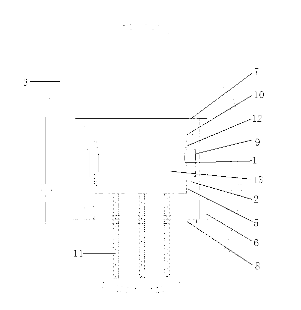
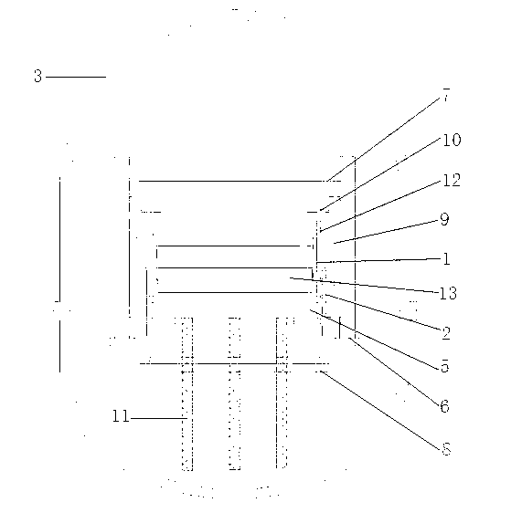
[0019] Such as Figure 2-3 As shown, a thermal field structure for casting polycrystalline silicon ingots includes a quartz crucible 1, a heat insulation plate 2, a side heater 9, a heat insulation layer 6, and a heat exchange table 5. The quartz crucible 1 is set on the heat exchange table 5. The outer wall is provided with a crucible guard plate 12, the quartz crucible 1 is surrounded by a heat insulation plate 2, and the outer side of the heat insulation plate 1 is provided with a side heat insulation layer 6, and a side heater is provided between the two 9. The distance between the outer wall of the heat insulation board 2 and the side heater 9 is greater than 1 cm, and the distance between the inner wall and the outer wall of the quartz crucible 1 is less than 5 cm, and the heat insulation board 2 is fixed on the side heat insulation layer 6 At the bottom, the upper part of the quartz crucible 1 is provided with an upper heat insulation layer 7, and the lower part is provided with a lower heat insulation layer 8, and an upper heater 10 is provided between the upper heat insulation layer 7 and the quartz crucible 1. The lower insulation layer 8 is fixed on the bracket 11. When the side insulation layer 6 descends, the insulation board 2 fixed on the side insulation layer 6 is driven to descend simultaneously, the side insulation layer 6 and the lower insulation layer 8 At this time, the upper heat insulation layer 7, the lower heat insulation layer 8, and the side heat insulation layer 6 form a closed state, and the top of the heat insulation plate 2 is located below the bottom of the quartz crucible 1; when the side heat insulation layer 6 rises At this time, the heat insulation board 2 rises accordingly. At this time, the upper heat insulation layer 7, the lower heat insulation layer 8, and the side heat insulation layer 6 are in an open state, the heat insulation board 2 is located at the upper limit, and the top of the heat insulation board 2 is located at the quartz crucible 1 above the bottom.
[0020] Place the quartz crucible 1 filled with silicon material 13 on the heat exchange table 5. When the side heat insulation layer 6 descends, the heat insulation plate 2 fixed on the side heat insulation layer 6 is driven to descend simultaneously, and the heat insulation plate 2 and The lower heat insulation layer 8 is connected. At this time, the upper heat insulation layer 7, the lower heat insulation layer 8, and the side heat insulation layer 6 form a closed state, and the space of the furnace wall 3 is evacuated, and the side heater 9 and The upper heater 10 heats the silicon material 13 in the quartz crucible 1. At this time, the height of the top of the heat insulation plate 2 at the lower limit is below the bottom of the quartz crucible 1, and has no heat insulation effect on the quartz crucible 1. When the silicon material 13 is completely After melting, the side heat insulation layer 6 rises, the silicon liquid 13 gradually solidifies from bottom to top, and the heat is radiated from the heat exchange platform 5, and the heat insulation board 2 rises with the side heat insulation layer 6 to keep the insulation The top of the hot plate 2 is 2 cm above and below the solid-liquid interface to reduce the thermal impact of the side heater 9 and the upper heater 10 on the crystal growth interface, stabilize the crystal growth and suppress the generation of crystal defects. At the same time, the heat shield 2 can also Isolate the first solidified silicon ingot from the heater to keep the temperature gradient in the middle and late stages of crystal growth constant, maintain the continuity of crystal growth, and reduce crystal defects.
[0021] After the silicon ingot is squared, it can be seen that the continuity of grain growth from bottom to top is better than that of conventional ingots, and the grain orientation is vertical upward. The small ingot is etched with HF+HNO3+H2O etching solution, which shows that the density of defects in the upper part of the silicon ingot is more conventional The ingot is significantly reduced. Compare the efficiency of the whole ingot silicon wafer before the transformation of the thermal field of the same furnace and the whole ingot silicon wafer of the present invention. The battery production line is offline at the same time. The battery efficiency comparison chart is as follows figure 1 Shown.

PUM

no PUM

Description & Claims & Application Information

We can also present the details of the Description, Claims and Application information to help users get a comprehensive understanding of the technical details of the patent, such as background art, summary of invention, brief description of drawings, description of embodiments, and other original content. On the other hand, users can also determine the specific scope of protection of the technology through the list of claims; as well as understand the changes in the life cycle of the technology with the presentation of the patent timeline. Login to view more.

Similar technology patents

Phase-change energy storage microcapsules and preparation method thereof

ActiveCN102977857AIncreased heating and cooling cycle lifereduce thermal shock
Owner:领致热能新电器(江苏)股份有限公司

Heat management module of engine cooling system and engine cooling system

InactiveCN111365113Asmall temperature fluctuationsReduce thermal shock
Owner:CHONGQING CHANGAN AUTOMOBILE CO LTD

Aluminum oxide feeding and concentration controlling method for aluminum electrolysis cell

PendingCN112575349Areduce thermal shockprevent concentration drift
Owner:SHENYANG ALUMINIUM MAGNESIUM INSTITUTE

Classification and recommendation of technical efficacy words

  • reduce thermal shock

Phase-change energy storage microcapsules and preparation method thereof

ActiveCN102977857AIncreased heating and cooling cycle lifereduce thermal shock
Owner:领致热能新电器(江苏)股份有限公司

Heat management module of engine cooling system and engine cooling system

InactiveCN111365113Asmall temperature fluctuationsReduce thermal shock
Owner:CHONGQING CHANGAN AUTOMOBILE CO LTD

Aluminum oxide feeding and concentration controlling method for aluminum electrolysis cell

PendingCN112575349Areduce thermal shockprevent concentration drift
Owner:SHENYANG ALUMINIUM MAGNESIUM INSTITUTE
Why Eureka
Try Eureka