
Level translation circuit

A technology for converting circuits and levels, applied in fail-safe circuits, logic circuit interface devices, logic circuit connection/interface layout, etc., can solve problems such as level conversion circuits not working normally, MOS tube breakdown, etc., to improve reliability performance, to ensure the effect of normal work

Pending Publication Date: 2018-06-29
上海安其威微电子科技有限公司
View PDF0 Cites 3 Cited by
  • Summary
  • Abstract
  • Description
  • Claims
  • Application Information

AI Technical Summary

Problems solved by technology

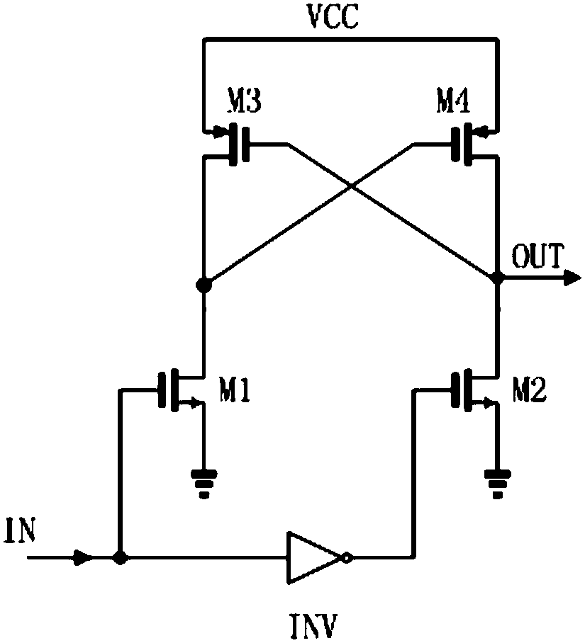
However, when the applied power supply voltage VCC exceeds the breakdown voltage of the MOS tube, figure 1 The MOS tube in the traditional level conversion circuit shown may be broken down, resulting in the level conversion circuit not working properly

Method used


Image

  • Level translation circuit
  • Level translation circuit
  • Level translation circuit

Examples


Embodiment Construction

[0019] Embodiments of the present invention are described in detail below with reference to the accompanying drawings.

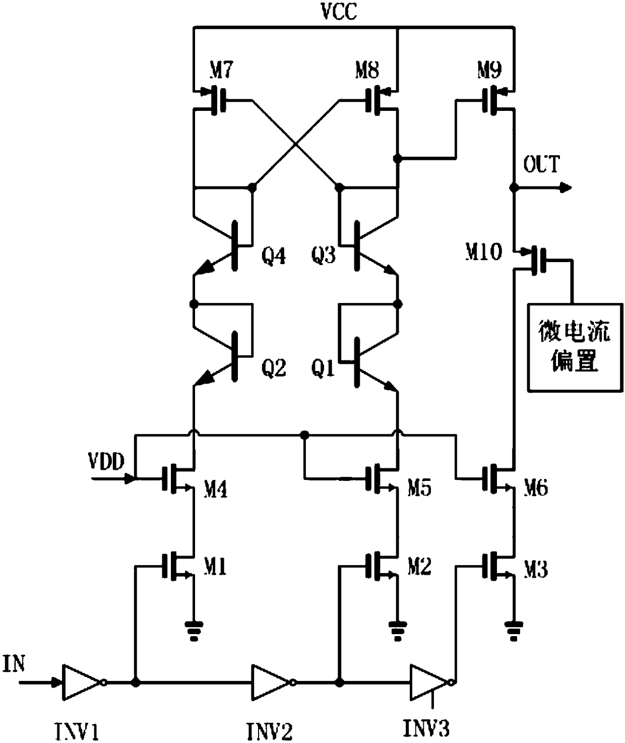
[0020] figure 2 A schematic structural diagram showing an example of the level conversion circuit provided by the embodiment of the present invention. figure 2 The level conversion circuit shown realizes the conversion of the input signal IN into the output signal OUT.

[0021] Such as figure 2 As shown, the level conversion circuit provided by the embodiment of the present invention includes a first NMOS transistor M1, a second NMOS transistor M2, a third NMOS transistor M3, a fourth NMOS transistor M4, a fifth NMOS transistor M5, and a sixth NMOS transistor M6 , the first PMOS transistor M7, the second PMOS transistor M8, the third PMOS transistor M9, the fourth PMOS transistor M10, the NPN transistor Q1, the NPN transistor Q2, the NPN transistor Q3, the NPN transistor Q4, the first inverter INV1, the second an inverter INV2, and a third inverter INV...


PUM


Abstract

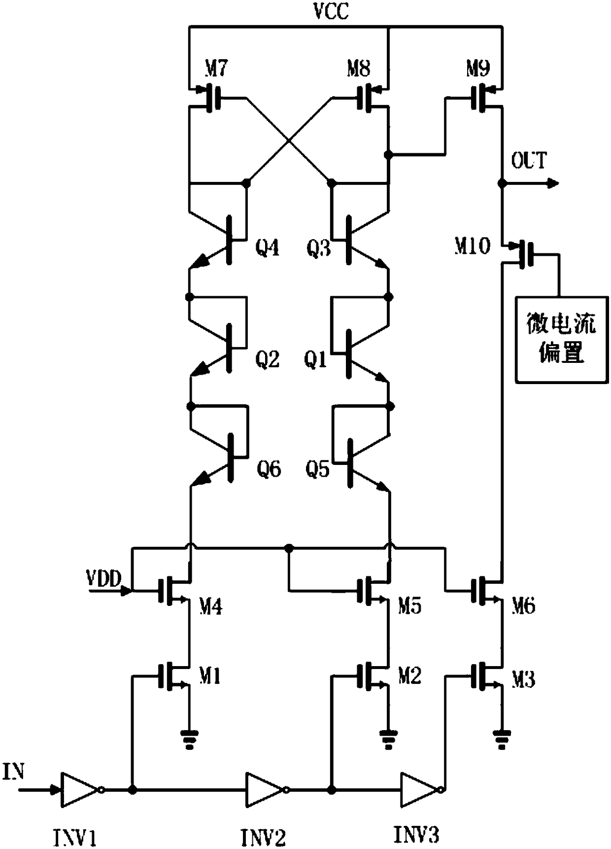
The invention discloses a level translation circuit. The circuit comprises a first phase inverter, a second phase inverter, a third phase inverter, a first NMOS tube, a second NMOS tube, a third NMOStube, a fourth NMOS tube, a fifth NMOS tube, a sixth NMOS tube, a first PMOS tube, a second PMOS tube, a primary NPN tube set, a third PMOS tube, and a fourth PMOS tube, wherein the primary NPN tube set comprises a first NPN tube and a second NPN tube. The level translation circuit can enable working points of all MOS tubes to not exceed the breakdown voltage thereof when the external power voltage of the level translation circuit exceeds the breakdown voltage of the internal MOS tube, thereby enabling the circuit to work in the safety working voltage range; the required level translation performance can be guarantee, and the circuit reliability can be improved to guarantee the normal work of the circuit.

Description

technical field [0001] The invention belongs to the field of integrated circuit design, and in particular relates to a level conversion circuit which realizes the level conversion function of BiCMOS technology and ensures that the working points of all MOS transistors do not exceed their breakdown withstand voltage values. Background technique [0002] Level conversion circuits are widely used in various interface circuits and input and output units to realize logic conversion of different levels. In the design of modern advanced BiCMOS integrated circuits, the internal circuit generally works at a lower voltage, such as 1.2V, 1.8V, while the external interface data voltage is relatively high, such as 3.3V, 5V, etc. Therefore, the level conversion circuit becomes one of the more critical circuits, which is responsible for raising the internal lower voltage to the external higher interface data voltage. [0003] figure 1 A schematic diagram showing the structure of a conven...

Claims


Application Information

Patent Timeline
IPC IPC(8): H03K19/0175H03K19/007
CPCH03K19/007H03K19/017509H03K19/01759
Inventor 陆建华马杰周帅林
Owner 上海安其威微电子科技有限公司
Learn More