ldmos device and its manufacturing method

A manufacturing method and device technology, applied in the fields of semiconductor/solid-state device manufacturing, semiconductor devices, electrical components, etc., can solve problems such as crosstalk control logic circuits, affecting product performance, noise interference, etc.

Active Publication Date: 2020-05-22
CSMC TECH FAB2 CO LTD
View PDF10 Cites 0 Cited by
  • Summary
  • Abstract
  • Description
  • Claims
  • Application Information

AI Technical Summary

Problems solved by technology

When the LDMOS device is working at high temperature, due to the electron-hole pairs generated by lattice scattering and collision, the leakage current generated will be collected by the substrate of the LDMOS device and flow around the substrate, which will cause the LDMOS device to control the peripheral logic circuit. Noise interference, crosstalk peripheral control logic circuits, affecting product performance

Method used


Image

  • ldmos device and its manufacturing method
  • ldmos device and its manufacturing method
  • ldmos device and its manufacturing method

Examples


Embodiment Construction

[0037] In order to facilitate the understanding of the present invention, the present invention will be described more fully below with reference to the associated drawings. Preferred embodiments of the invention are shown in the accompanying drawings. However, the present invention can be embodied in many different forms and is not limited to the embodiments described herein. On the contrary, these embodiments are provided to make the understanding of the disclosure of the present invention more thorough and comprehensive.

[0038] Unless otherwise defined, all technical and scientific terms used herein have the same meaning as commonly understood by one of ordinary skill in the technical field of the invention. The terms used herein in the description of the present invention are for the purpose of describing specific embodiments only, and are not intended to limit the present invention. As used herein, the term "and / or" includes any and all combinations of one or more of ...


PUM


Abstract

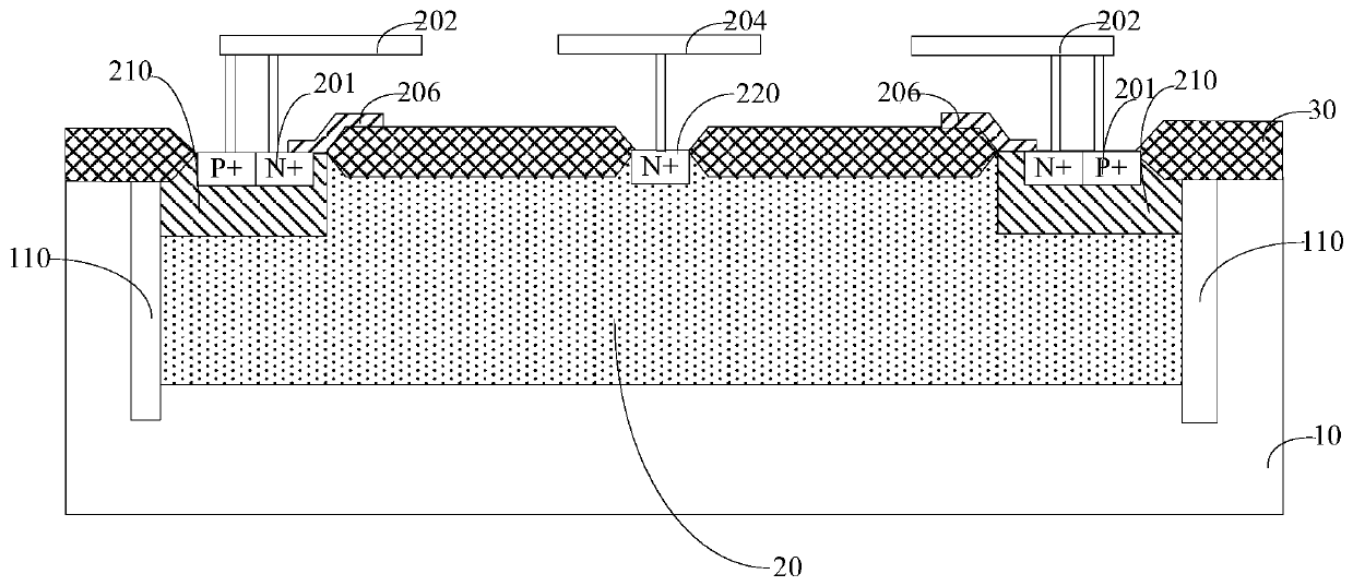
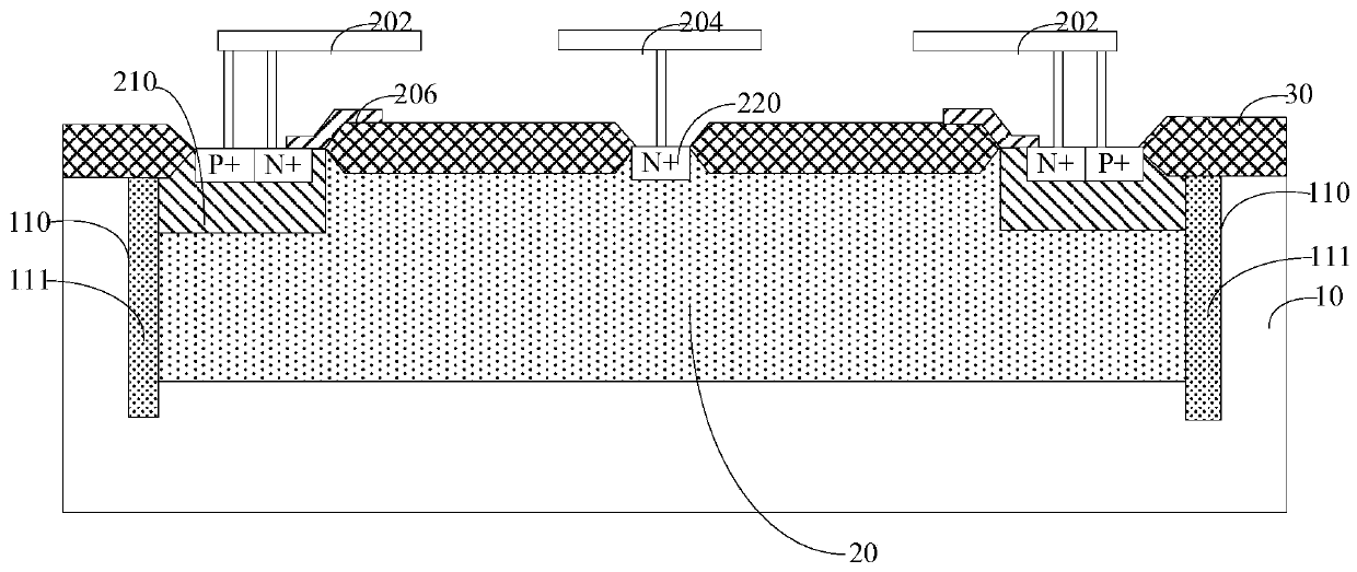
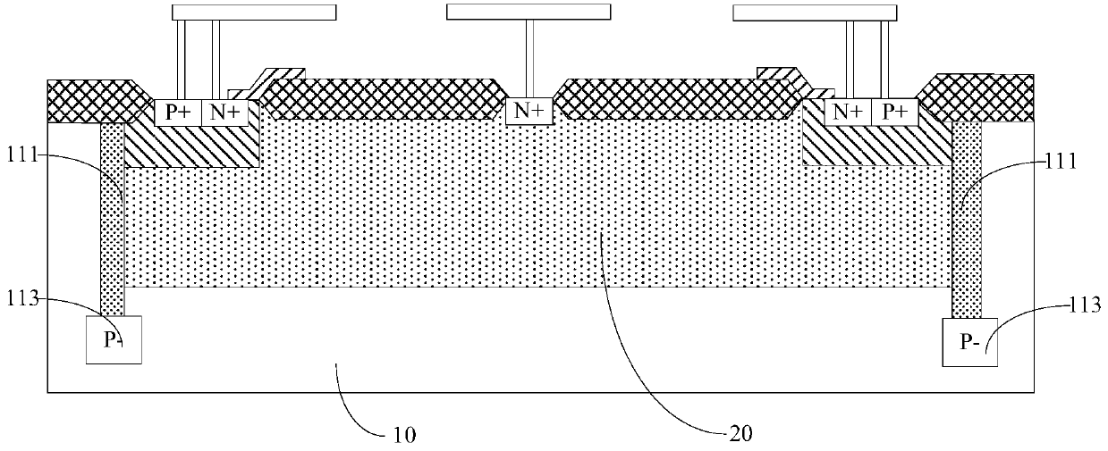
The invention relates to an LDMOS device and a manufacturing method thereof. An LDMOS device comprising a substrate, a drift region on the substrate, the drift region including a source region and a drain region; and a trench surrounding the drift region, the depth of the trench being greater than that of the drift region depth. Because its trench surrounds the drift region, it can limit the hole current in the electron-hole pairs generated by the LDMOS device at high temperature from flowing to the substrate, that is, it can effectively isolate the LDMOS device from the peripheral logic circuit and avoid the occurrence of crosstalk. In addition, a manufacturing method of the LDMOS device is also provided.

Description

technical field [0001] The invention relates to the technical field of semiconductors, in particular to an LDMOS device and a manufacturing method thereof. Background technique [0002] The manufacture of Lateral Double-diffuse MOS (LDMOS) devices mainly uses double-diffusion technology, and two boron-phosphorus diffusions are performed successively in the same active area. The difference in lateral junction depth is used to precisely control the length of the channel. At the same time, the drift region acts as a buffer between the channel and the drain, weakening the short channel effect of the LDMOS device. [0003] Traditional high-voltage power LDMOS devices are usually formed using Double-RESURF (reduced surface electric field) technology. Double-RESURF technology is to introduce a doped region opposite to the conductivity type of the drift region in the middle surface of the drift region of the device to improve the surface of the drift region. The electric field dis...

Claims


Application Information

Patent Timeline
Patent Type & Authority Patents(China)
IPC IPC(8): H01L29/78H01L29/06H01L21/336
CPCH01L29/06H01L29/66681H01L29/78H01L29/7816H01L29/42368H01L29/0634
Inventor 张广胜张森胡小龙
Owner CSMC TECH FAB2 CO LTD
Why Eureka
Try Eureka