
Focal plane array detector and preparation method thereof

A technology of focal plane array and detector, which is applied in the field of focal plane array detector and its preparation, can solve the problems of small effective use area of ​​pixels, easy crosstalk of PN junction, weak photoelectric signal, etc., to solve the problem of weak photoelectric signal, Realize the effect of easy process and simple operation

Active Publication Date: 2018-07-06
WUHAN GAOXIN TECH
View PDF3 Cites 11 Cited by
  • Summary
  • Abstract
  • Description
  • Claims
  • Application Information

AI Technical Summary

Problems solved by technology

[0004] In view of the above defects or improvement needs of the prior art, the present invention provides a focal plane array detector, the purpose of which is to solve the problem that the PN junctions of adjacent pixels are easy to crosstalk, and the effective use area of ​​the pixels is small, which leads to the collection of photoelectric signals. Faint, technical problem with too low signal-to-noise ratio

Method used


Image

  • Focal plane array detector and preparation method thereof
  • Focal plane array detector and preparation method thereof
  • Focal plane array detector and preparation method thereof

Examples


Embodiment Construction

[0039] In order to make the object, technical solution and advantages of the present invention clearer, the present invention will be further described in detail below in conjunction with the accompanying drawings and embodiments. It should be understood that the specific embodiments described here are only used to explain the present invention, not to limit the present invention. In addition, the technical features involved in the various embodiments of the present invention described below can be combined with each other as long as they do not constitute a conflict with each other.

[0040] It should be noted that, in the description of the present invention, the terms "up", "down", "front", "rear", "left", "right", "vertical", "horizontal", etc. indicate directions or The positional relationship is based on the orientation or positional relationship shown in the drawings, which is only for the convenience of describing the present invention and simplifying the description, ...


PUM


Abstract

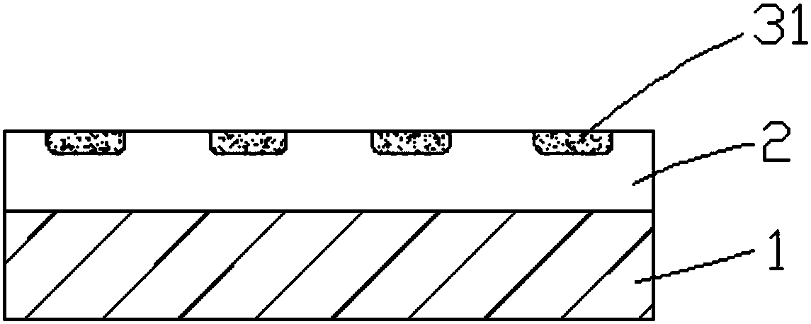
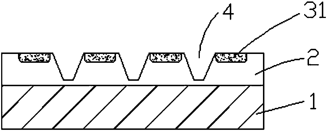
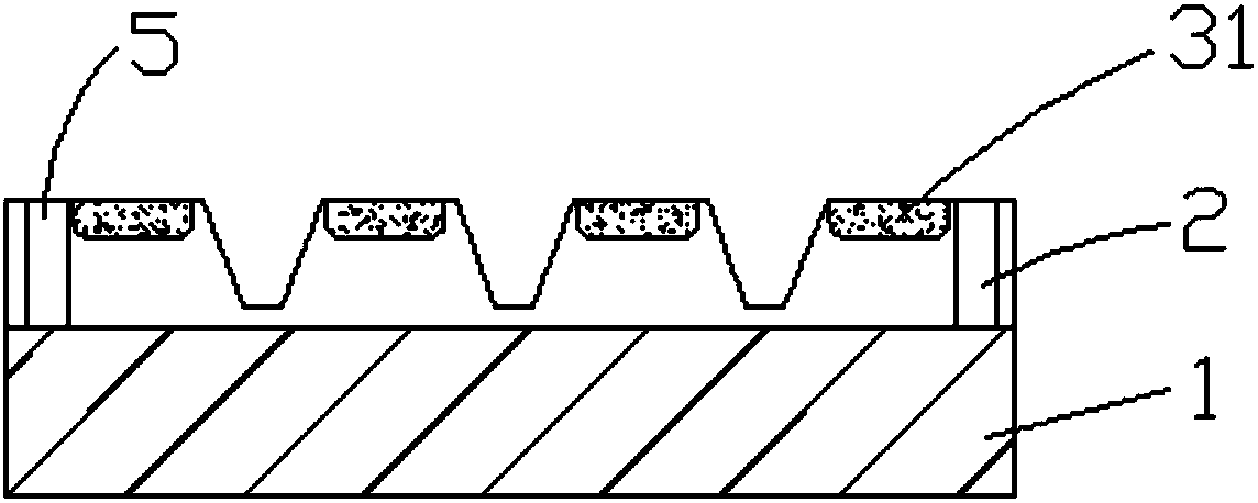
The invention discloses a focal plane array detector and a preparation method thereof. The focal plane array detector comprises an epitaxial layer. The lower surface of the epitaxial layer is providedwith multiple concave first doped regions. The interfaces of the epitaxial layer and the first doped regions are first PN junctions. A pixel element hole is arranged between the adjacent first PN junctions. The lower surface of the epitaxial layer is covered by a first passivation film. The first passivation film arranged on the surface of the first doped regions is provided with first contact holes. The exact middle of the first passivation film arranged on the surface of the pixel element holes is provided with second contact holes. The first contact holes and the second contact holes are filled with first indium bumps and second indium bumps respectively. The first indium bumps and the second indium bumps protrude out of the epitaxial layer. The upper surface of the epitaxial layer isprovided with multiple concave second doped regions. The first doped regions and the second indium bumps are connected in a one-to-one correspondence way. The objective of the invention is to solve the technical problems of crosstalk of the PN junctions of the adjacent pixel elements and small effective utilization area of the pixel elements.

Description

technical field [0001] The invention belongs to the field of optoelectronic technology, and more specifically relates to a focal plane array detector and a preparation method thereof. Background technique [0002] Like silicon-based semiconductors, focal plane array detectors are developing in the direction of small size and high integration. However, due to the particularity of the material, its processing difficulty and technical bottleneck have seriously hindered the further development of the focal plane array detector technology. In particular, there is a problem of crosstalk between the PN junctions of adjacent pixels. Traditionally, the PN junctions of adjacent pixels are distributed in a planar manner, that is, adjacent PN junctions are located on the same horizontal plane. In order to prevent adjacent PN junctions from If the spacing is too small, crosstalk is caused, and the spacing between adjacent PN junctions is relatively large, which limits the utilization of...

Claims


Application Information

Patent Timeline
Patent Type & Authority Applications(China)
IPC IPC(8): H01L27/146G01J1/42
CPCG01J1/42H01L27/14607H01L27/1461H01L27/14636H01L27/14683
Inventor 金迎春刘斌周文洪黄立
Owner WUHAN GAOXIN TECH
Learn More