Image sensor and forming method thereof

An image sensor and patterning technology, which is applied in the direction of electric solid-state devices, semiconductor devices, electrical components, etc., can solve the problems of low full well capacity, electrical crosstalk, and insufficient DTI depth, etc., to improve full well capacity, increase thickness, reduce Effects of Electrical Crosstalk

Inactive Publication Date: 2018-07-13
HUAIAN IMAGING DEVICE MFGR CORP
View PDF3 Cites 4 Cited by
  • Summary
  • Abstract
  • Description
  • Claims
  • Application Information

AI Technical Summary

Problems solved by technology

[0005] However, in the above two technologies, there is a problem of insufficient DTI depth, which leads to serious electrical crosstalk; and due to the limitation of DTI depth, the thickness of the photodiode is not enough, resulting in the problem that the full well capacity is too low

Method used


Image

  • Image sensor and forming method thereof
  • Image sensor and forming method thereof
  • Image sensor and forming method thereof

Examples


Embodiment Construction

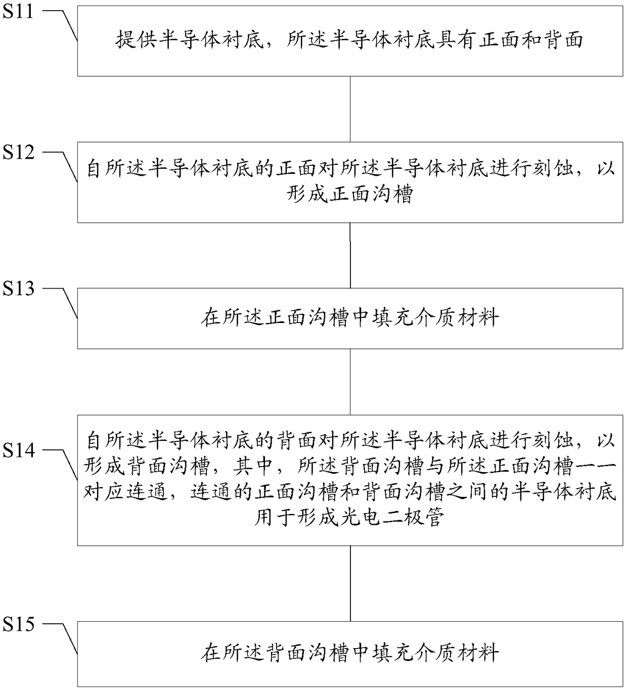
[0022] In the prior art, in order to prevent photocarriers in different regions from diffusing to adjacent regions, it is necessary to form DTI inside the semiconductor substrate. However, due to the insufficient depth of the DTI, serious electrical crosstalk is caused, and due to the limitation of the depth of the DTI, the thickness of the photodiode is insufficient, resulting in a too low full well capacity. Specifically, full well capacity is the maximum charge a pixel can hold before saturation leading to signal degradation. When the charge in a pixel exceeds the saturation level, the charge begins to fill adjacent pixels, a process known as blooming.

[0023] The inventors of the present invention have found through research that in the prior art, DTI is only formed on one side of a semiconductor substrate, and it is difficult to form a very deep DTI due to the limitation of existing process capabilities. Specifically, for example, it is difficult to form very deep DTI t...


PUM


Abstract

The invention discloses an image sensor and a forming method thereof. The method includes steps of providing a semiconductor substrate, wherein the semiconductor substrate comprises a front face and aback face; etching the semiconductor substrate from the front face of the semiconductor substrate to form a front groove, filling a medium material in the front groove; etching the semiconductor substrate from the back face of the semiconductor substrate to form a back groove, wherein the back groove is correspondingly connected with the front groove; the semiconductor substrate between the connected front groove and the back groove is used for forming a photodiode; filling the medium material in the back channel. The scheme can effectively reduce the electricity crosstalk, improve the thickness of the photodiode, and further improve the full trap capacity.

Description

technical field [0001] The invention relates to the technical field of semiconductor manufacturing, in particular to an image sensor and a forming method thereof. Background technique [0002] The image sensor is the core component of the camera equipment, which realizes the image capture function by converting the optical signal into an electrical signal. Taking CMOS Image Sensors (CIS) devices as an example, in the manufacturing process, in order to prevent the photogenerated carriers in different regions from diffusing to adjacent regions, it is necessary to form Deep Trench Isolation (Deep Trench Isolation, DTI). [0003] In one prior art, after active devices are formed on the front side of the semiconductor substrate of a device wafer (Device Wafer), DTI can be formed on the back side of the semiconductor substrate. Specifically, the semiconductor substrate is etched from the back of the semiconductor substrate to form a trench, and then a dielectric material is fill...

Claims


Application Information

Patent Timeline
Patent Type & Authority Applications(China)
IPC IPC(8): H01L27/146
CPCH01L27/1463H01L27/14687
Inventor 王连红黄晓橹
Owner HUAIAN IMAGING DEVICE MFGR CORP
Why Eureka
Try Eureka