Optical fiber assembly applied to silicon photonic optical communication

A technology for optical fiber components and optical communication, which is applied in the coupling of optical components, optical waveguides, and light guides. Small, the effect of reducing material cost and production cost

Inactive Publication Date: 2018-07-27
BROADEX TECH
View PDF10 Cites 3 Cited by
  • Summary
  • Abstract
  • Description
  • Claims
  • Application Information

AI Technical Summary

Problems solved by technology

However, since the mode field diameter of the silicon photonic chip is only 3.0-4.0um or smaller, while the mode field diameter of the conventional optical fiber component is 9-10um, in order to reduce the coupling loss and meet the transmission requirements, the current process is to combine the silicon photonic chip and The fiber optic components are coupled through lens focusing ( image 3 ), this process cannot really meet the requirements of low manufacturing cost and high-density integration of silicon photonic devices

Method used


Image

  • Optical fiber assembly applied to silicon photonic optical communication
  • Optical fiber assembly applied to silicon photonic optical communication
  • Optical fiber assembly applied to silicon photonic optical communication

Examples


Embodiment Construction

[0026] Below in conjunction with specific embodiment, further illustrate the present invention. It should be understood that these examples are only used to illustrate the present invention and are not intended to limit the scope of the present invention. In addition, it should be understood that after reading the teachings of the present invention, those skilled in the art can make various changes or modifications to the present invention, and these equivalent forms also fall within the scope defined by the appended claims of the present application.

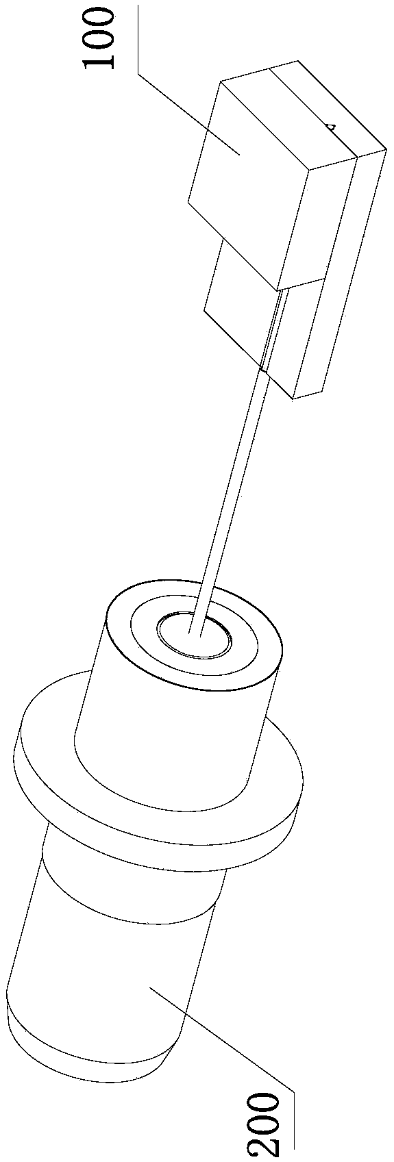
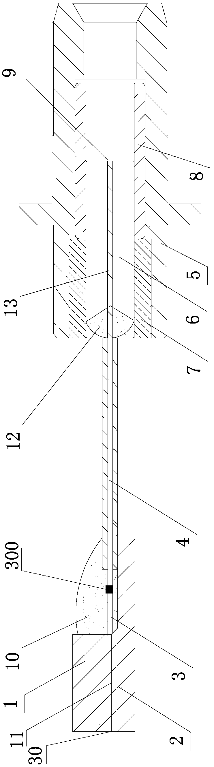
[0027] Embodiments of the present invention relate to optical fiber assemblies applied to silicon photonic optical communications, such as figure 1 with figure 2 As shown, an optical fiber array unit 100 and a ferrule assembly 200 are included. The fiber array unit includes a coupling end face 10 , a glass cover 1 , a glass substrate 2 , a small mode field fiber 3 , and a conventional field fiber 4 . After the small-mode-f...


PUM


Abstract

The invention provides an optical fiber assembly applied to silicon photonic optical communication. The optical fiber assembly comprises an optical fiber array unit and a core inserting assembly. Theoptical fiber array unit comprises a coupling end surface, a glass cover plate, a glass substrate, a small-mode-field optical fiber and a normal-scale-field optical fiber. The small-mode-field opticalfiber is connected with the normal-scale-field optical fiber in a welding mode. The small-mode-field optical fiber is fixed between the glass cover plate and the glass substrate, and the end surfaceof the small-mode-field optical fiber is polished to form the coupling end surface of the optical fiber array unit. The normal-scale-field optical fiber at the other end of the optical fiber array unit is assembled into the core inserting assembly. According to the invention, the optical fiber assembly is low in manufacturing cost. Through the fusion welding of optical fibers of different mode-field diameters, the small-mode-field optical fiber can be directly connected with a silicon optical chip. Since no lens is required, the assembling difficulty is reduced. Meanwhile, the optical fiber assembly is high in assembling efficiency and small in size. The transmission performance of optical signals can be ensured.

Description

technical field [0001] The invention relates to silicon photonic optical communication, in particular to input and output optical fiber components of silicon photonic devices. Background technique [0002] Silicon photonics technology, which uses laser beams instead of electronic signals to transmit data, combines optical and electronic components into a single microchip to speed up chip-to-chip connections between routers and switch line cards. Using light as an information transmission medium on a silicon chip can achieve better data transmission performance than traditional copper wires and reduce energy consumption. Optical fiber components are key components for data input and output of silicon photonic devices, and the innovation of their technical solutions is the key to breaking through the bottleneck of silicon photonic device production. With the deployment of data centers and mobile 4G and 5G networks, increasingly stringent requirements are placed on the transmi...

Claims


Application Information

Patent Timeline
Patent Type & Authority Applications(China)
IPC IPC(8): G02B6/255G02B6/26G02B6/38
CPCG02B6/2551G02B6/262G02B6/3807
Inventor 杨佳捷
Owner BROADEX TECH
Why Eureka
Try Eureka